5 Troubleshooting
5-6
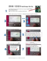
5-4 No Picture (Tuner_CVBS)
Dose the signal
appear at #14 of IC203?
Check a B+ voltage (#7 of Tuner) :
5V change a main PCB ass'y
Yes
Does the signal appear at
#13 of IC203?
Check a IC203.
Change a main PCB ass'y.
Yes
Does the digital data appear at
output of FT250~FT253 ?
Check a IC201.
Change a main PCB ass'y.
Yes
Power Indicator is off.
Lamp on, no picure.
No
Connect the RF cable and
check RF signal.
No
No
No
Yes
Check a LVDS cable?
Replacea lcd panel?
Please, Call to Samsung Co. LTD.
No
5
5
3
Summary of Contents for LE26R51B
Page 7: ...4 Alignments and Adjustments 4 3 ...
Page 8: ...4 Alignments and Adjustments 4 4 ...
Page 9: ...4 Alignments and Adjustments 4 5 ...
Page 10: ...4 Alignments and Adjustments 4 6 ...
Page 16: ...8 Block Diagrams 8 2 Memo ...
Page 23: ...10 PCB Layout 10 1 10 PCB Layout ...
Page 33: ...2 Product Specifications 2 9 2 6 1 Supported Modes 1 ...
Page 34: ...2 Product Specifications 2 10 2 6 1 Supported Modes 2 ...
Page 35: ...2 Product Specifications 2 11 2 6 1 Supported Modes 3 ...
Page 36: ...Memo 2 Product Specifications 2 12 ...
Page 41: ...5 Troubleshooting 5 5 WAVEFORMS 3 Digital Output Data of IC201 4 Signal of HDMI Data ...
Page 43: ...5 Troubleshooting 5 7 WAVEFORMS 3 Digital Output Data of IC201 5 Tuner_CVBS Output Signal ...
Page 45: ...5 Troubleshooting 5 9 WAVEFORMS 3 Digital Output Data of IC515 5 Tuner_CVBS Output Signal ...
Page 47: ...5 Troubleshooting 5 11 3 Digital Output Data of IC201 6 Analog Signal Y C to IC201 WAVEFORMS ...
Page 49: ...5 Troubleshooting 5 13 WAVEFORMS 7 The Signal are Inputed to IC610 8 DC 8V 9 Output WaveForm ...
Page 50: ...Memo 5 Troubleshooting 5 14 ...
Page 80: ...9 Wiring Diagrams 9 2 9 2 Main Board Layout Except for 23 Except for 23 Except for 23 ...
Page 81: ...9 2 PIN characteristic 9 Wiring Diagrams 9 3 ...
Page 82: ...9 Wiring Diagrams 9 4 ...
Page 83: ...9 Wiring Diagrams 9 5 9 3 Power Board Layout ...
Page 84: ...9 Wiring Diagrams 9 6 ...
Page 86: ...11 Schematic Diagrams 11 2 11 2 In_Out_Jack Schematic Diagram ...
Page 87: ...11 3 11 Schematic Diagrams 11 3 MICOM Schematic Diagram 1 R G B Output Signal of IC906 ...