

LE15E31S
9-1
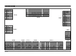
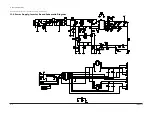
9 Wiring Diagram
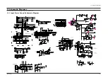
CN703
CN601
CN600
CN907
CN902
CN903
CN100
GND
SW_Inverter
GND
5V
5V
-
GND
GND
14V
14V
GND
5V
5V
GND
GND
TX0
TX0
GND
TX1
TX1
GND
TX2
TX2
GND
TX3
TX3
GND
TX4
TX4
GND
-
+
+
+
+
+
-
-
-
-
-
1
2
3
4
GND
GND
OUT
-R
OUT
-R
1
2
3
4
GND
OUT
-L
-
OUT
-L
1
2
3
4
GND
5
GND
Sound L
out
Sound R In
Sound R out
1
2
3
4
GND
5
ID
Cb
Sound L
In
6
GND
GND
S_V
ideo_Y
S_V
ideo_C
1
2
3
4
GND
5
-
6
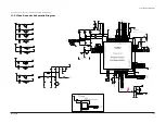
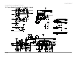
U1913
CN900
CN908
GND
Audio-R
Audio-R
GND
1
2
3
VIdeo-CVBS
V
ideo-CVBS
GND
1
2
3
4
Audio-L
5
Audio-L
6
7
8
GND
NC
Y
NC
GND
GND
Cr
BL
In
GND
GND
V
ideo Out
V
ideo In
GND
9
10
11
12
13
14
15
16
17
18
19
20
21
5
6
7
8
9
10
11
12
13
14
15
16
17
18
19
20
21
22
1
2
3
4
5
6
7
8
9
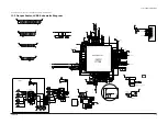
LED-GRN
LED-RED
-
3.3V
IR
GND
IDENT_HP
HP-L
HP-R
1
2
3
4
5
6
7
8
9
GND
KEY 1
KEY 2
10
11
12
GND
GND
13
14
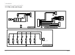
CN909
GND
PC_AR
PC_AL
PC_AL
PC_AL
PC_AR
PC_AR
4
5
6
7
8
9
10
PC_SCL
D SUB_V
D SUB_H
PC_SDA
GND
IDENT_PC
DC_5V
GND
GND
GND
GND
GND
PC_Blue
PC_Green
PC_Red
1
2
3
4
5
6
7
8
9
10
11
12
13
14
15


