Reference Information
Samsung Electronics
2-3
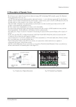
2-2 Description of Dynamic Focus
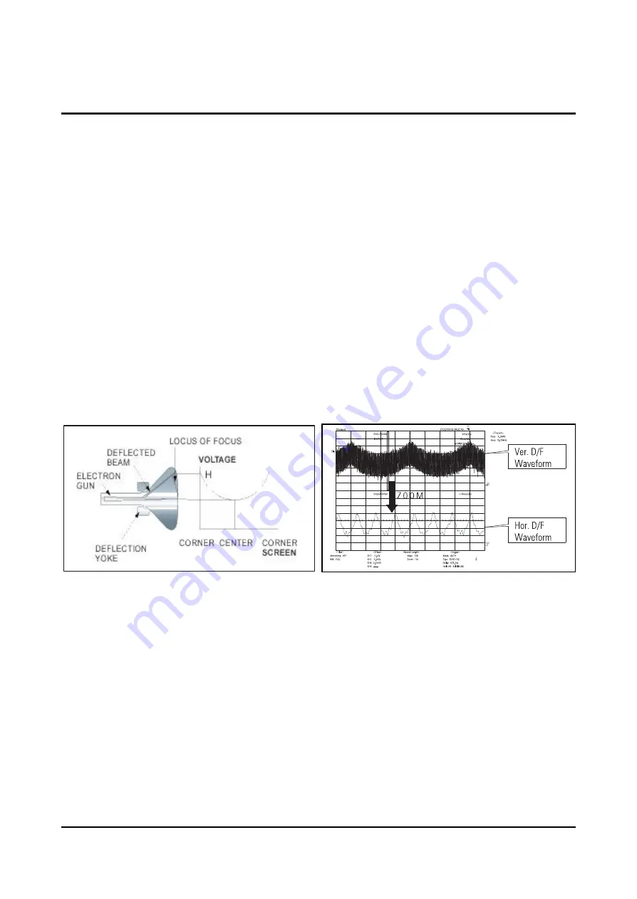
Most large-screen video display devices that are using CRT (including CDT) usually apply the Dynamic
Focus (hereinafter D/F) circuit.
As CRT has non-spherical surface (perfect spherical surface = 1, non-spherical surface R>1), the distance
that the electron beam emitted from the electron gun reaches to the center of CRT is different from the one
that the electron beam reaches to the corners. (See Figure 1.)
Only the beam, which has the equal distance as the beam from the electron gun to the center of CRT
surface, can maintain the optimum focus.
By this reason, focus dagradation at corners occurs inevitably.
To recover this, the speed of the electron beam injected into the corners of CRT should increase and the
focus dagradation by the difference of distances can be compensated.
Increasing the voltage is used as a method of increasing the speed of the electron beam at the corners of
screen.
In this case, an ideal D/F voltage waveform is the form of parabola where the center of screen has low
voltage and the corners has the highest voltages.
The horizontal D/F waveform compensates the focus dagradation at left and right sides, but the vertical
D/F waveform does at top and bottom sides.
The horizontal D/F and vertical D/F waveforms are separately created and mix two signals to
compensate the focus of the whole screen.
And the vertical Dynamic Focus waveform is composed of the horizontal Dynamic Focus waveforms as
much as the number of scanning lines. (See Figure 2.)
Fig. 1 Dynamic Focus Diagram (Horizantal)
Fig. 2 H/V Dynamic Focus Waveform
Summary of Contents for HCN5527WX/XAA
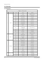
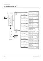
Page 9: ...Reference Information 2 4 Samsung Electronics 2 3 IC Line Up 2 3 1 Progressive...
Page 10: ...Reference Information Samsung Electronics 2 5...
Page 11: ...Reference Information 2 6 Samsung Electronics 2 4 MICOM IIC BUS LINE UP...
Page 13: ...MEMO 3 2 Samsung Electronics...
Page 51: ...MEMO 4 38 Samsung Electronics...
Page 55: ...MEMO 5 4 Samsung Electronics...
Page 69: ...7 12 Samsung Electronics MEMO...
Page 79: ...Schematic Diagrams 10 2 Samsung Electronics TP20 TP03 TP04 10 2 MAIN 2 TP03 TP04 TP20...
Page 80: ...Samsung Electronics Schematic Diagrams 10 3 10 3 MAIN 3 TP12 TP13 TP12 TP13...
Page 82: ...Samsung Electronics Schematic Diagrams 10 5 10 5 MICOM...
Page 83: ...Schematic Diagrams 10 6 Samsung Electronics 10 6 CRT...
Page 84: ...Samsung Electronics Schematic Diagrams 10 7 10 7 SUB 1 TP21 TP21...
Page 85: ...Schematic Diagrams 10 8 Samsung Electronics 10 8 SUB 2 TP24 TP23 TP22 TP22 TP23 TP24...
Page 86: ...Samsung Electronics Schematic Diagrams 10 9 10 9 CONVERGENCE SDC12 1...
Page 87: ...Schematic Diagrams 10 10 Samsung Electronics 10 10 CONVERGENCE SDC12 2...
Page 88: ...Samsung Electronics Schematic Diagrams 10 11 10 11 PRO SCAN 1...
Page 89: ...Schematic Diagrams 10 12 Samsung Electronics 10 12 PRO SCAN 2...
Page 90: ...Samsung Electronics Schematic Diagrams 10 13 10 13 PRO SCAN 3...
Page 91: ...Schematic Diagrams 10 14 Samsung Electronics 10 14 PRO SCAN 4...
Page 92: ...10 15 CG AMP Samsung Electronics Schematic Diagrams 10 15...
Page 93: ...Schematic Diagrams 10 16 Samsung Electronics 10 16 AV FRONT...
Page 94: ...10 17 CONTROL Samsung Electronics Schematic Diagrams 10 17...
Page 95: ...Schematic Diagrams 10 18 Samsung Electronics 10 18 DY JACK SENSOR DY JACK SENSOR...


