background image

SAMSUNG Proprietary-Contents may change without notice

11. Disassembly and Assembly Instructions

11-1

This Document can not be used without Samsung's authorization

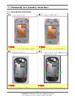
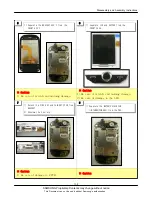
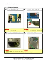
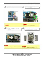
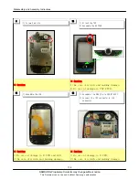
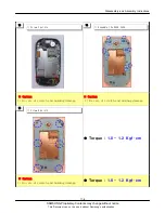
※ Caution

1) Be care of scratch and molding damage.

※ Caution

1) Be care of scratch and molding damage.

※ Caution

1) Be care of damage to INTENNA

※ Caution

1) Be care of scratch and molding damage.

11-1. Disassembly Instructions

1) Unscrew the 6 points.

1

1) Unscrew the 2 points.

2

3

4

1) Seperate the REAR CASE.

1) Separate the LCD and TSP CONNECTORS then

disassemble the 2 hook.

Summary of Contents for GT-M3710L

Page 1: ...recautions 2 Specification 3 Product Function 4 Array course control 5 Exploded View and Parts List 6 Main Electrical Parts List 7 Block Diagrams 8 PCB Diagrams 9 Flow Chart of Troubleshooting 10 Reference data 11 Disassembly and Assembly instructions efrcom ...

Page 2: ...ngportal com Europe europe samsungportal com China china samsungportal com Asia asia samsungportal com Mideast Africa mea samsungportal com This Service Manual is a property of Samsung Electronics Co Ltd Any unauthorized use of Manual can be punished under applicable International and or domestic law Samsung Electronics Co Ltd 2010 02 Rev 1 0 ⓒ ...

Page 3: ... PAM100 IC 1203 006077 U500 IC 1203 006176 U304 IC 1205 003656 UCP200 IC 1205 003839 U106 IC 1205 003868 U101 IC 1404 001221 VR200 THERMISTOR 2007 000137 R501 R CHIP 2007 000138 R109 R219 R303 R318 R CHIP 2007 000138 R414 R CHIP 2007 000140 R406 R CHIP 2007 000143 R200 R203 R204 R216 R CHIP 2007 000143 R217 R417 R421 R422 R CHIP 2007 000144 R207 R208 R209 R210 R CHIP 2007 000144 R308 R CHIP 2007 0...

Page 4: ... C305 C306 C308 C357 C CERAMIC CHIP 2203 000386 C501 ZD401 ZD402 C CERAMIC CHIP 2203 000425 C218 C CERAMIC CHIP 2203 000438 C234 C CERAMIC CHIP 2203 000550 C302 C304 C CERAMIC CHIP 2203 000679 C229 C423 C CERAMIC CHIP 2203 000696 C147 C CERAMIC CHIP 2203 000812 C118 C119 C355 C400 C CERAMIC CHIP 2203 000812 L107 L111 C CERAMIC CHIP 2203 000854 C226 C233 C CERAMIC CHIP 2203 000995 C204 C215 C230 C4...

Page 5: ...3 006399 C340 C341 C342 C345 C CERAMIC CHIP 2203 006399 C356 C513 C515 C521 C CERAMIC CHIP 2203 006399 C522 C CERAMIC CHIP 2203 006562 C141 C142 C301 C323 C CERAMIC CHIP 2203 006562 C333 C509 C514 C CERAMIC CHIP 2203 006681 C213 C214 C224 C228 C CERAMIC CHIP 2203 006681 C422 C CERAMIC CHIP 2203 006824 C101 C CERAMIC CHIP 2203 006825 C335 C CERAMIC CHIP 2203 006838 C100 C CERAMIC CHIP 2203 006841 C...

Page 6: ...C200 CRYSTAL UNIT 2901 001435 F500 F501 F502 FILTER EMI 2904 001935 F101 FILTER SAW 2904 001936 F100 FILTER SAW 2909 001299 F102 FILTER DUPLEXER 3003 001138 MIC400 MIC401 MIC CONDENSOR 3301 001438 L126 CORE FERRITE 3301 001534 L100 L101 CORE FERRITE 3301 001659 L123 L124 L200 L202 CORE FERRITE 3301 001885 L402 L403 L404 L409 CORE FERRITE 3301 001885 L410 L500 L503 L504 CORE FERRITE 3705 001503 RFS...

Page 7: ...eck the VBAT more than 3 3V No Check the Battery Yes Check the related circuit No C301 VBAT 3 0V Yes Check the U304 and L301 No Check the MEM_1 8V of U304 is more than 1 8V 1 8V Yes Check U304 3 0V_DIG 3 0V 3 0V_ANLG 3 0V 1 2V_ANLG 1 2V No Check the U304 and C328 C329 C347 Yes Yes Yes Check the clock 32KHz_DIGIT No Check CLK32K Freq 32KHz Check the initial operation END Check the current consumpti...

Page 8: ... O O D D L L S S M M 5 5 B B 2 2 O O D D L L S S M M 6 6 B B 2 2 O O D D L L A A 7 7 B B 7 7 N N I I 1 1 A A 1 1 X X L L 2 2 A A 1 1 N N I I 3 3 A A O O D D L L O O I I 4 4 A A 2 2 O O D D L L C C H H 5 5 A A 1 1 O O D D L L C C H H 6 6 A A 2 2 O O D D L L F F R R 7 7 A A 1 1 O O D D L L F F R R 8 8 A A C C N N 4 4 0 0 3 3 U U C C N N 1 1 C C N N 2 2 C C N N 3 3 1 1 3 3 C C 7 7 4 4 3 3 C C 9 9 2 2...

Page 9: ...This Document can not be used without Samsung s authorization Flow Chart of Troubleshooting 9 3 9 2 Initial Initial Failure Yes U304 pin E3 RESETB H check the test point No Check the circuit related to reset Yes Check the 16bit data signal memory CE END Yes ...

Page 10: ... O O D D L L S S M M 5 5 B B 2 2 O O D D L L S S M M 6 6 B B 2 2 O O D D L L A A 7 7 B B 7 7 N N I I 1 1 A A 1 1 X X L L 2 2 A A 1 1 N N I I 3 3 A A O O D D L L O O I I 4 4 A A 2 2 O O D D L L C C H H 5 5 A A 1 1 O O D D L L C C H H 6 6 A A 2 2 O O D D L L F F R R 7 7 A A 1 1 O O D D L L F F R R 8 8 A A C C N N 4 4 0 0 3 3 U U C C N N 1 1 C C N N 2 2 C C N N 3 3 1 1 3 3 C C 7 7 4 4 3 3 C C 9 9 2 2...

Page 11: ...g s authorization Flow Chart of Troubleshooting 9 5 9 3 Charging Part Yes Resolder or replace U304 Check the circuit related to ACC_DET signal Check the circuit related to VBUS_5V_IF Yes No Check the U304 pin D5 1 25V Yes No C322 ACC_DET L Yes No END Abnormal charging part Check the U304 pin E9 5 0V ...

Page 12: ... O O D D L L S S M M 5 5 B B 2 2 O O D D L L S S M M 6 6 B B 2 2 O O D D L L A A 7 7 B B 7 7 N N I I 1 1 A A 1 1 X X L L 2 2 A A 1 1 N N I I 3 3 A A O O D D L L O O I I 4 4 A A 2 2 O O D D L L C C H H 5 5 A A 1 1 O O D D L L C C H H 6 6 A A 2 2 O O D D L L F F R R 7 7 A A 1 1 O O D D L L F F R R 8 8 A A C C N N 4 4 0 0 3 3 U U C C N N 1 1 C C N N 2 2 C C N N 3 3 1 1 3 3 C C 7 7 4 4 3 3 C C 9 9 2 2...

Page 13: ...w Chart of Troubleshooting 9 7 9 4 Sim Part Phone can t access SIM Card Yes Check the SIMVCC 3 0V No Check the circuit related to R311 C340 Yes Check the SIM connector s connector s to SIM card resolder or change SIM300 No Yes Check the related circuit of SIM300 No Check the circuit around SIM300 input circuitry Yes END ...

Page 14: ...11 R316 R317 RTCK 0 0 1 C S SIM300 TCK TDI TDO TMS TP220 TRSTB R R O O T T C C E E N N N N O O C C M M I I S S 9 9 3 3 3 3 C C 4 4 4 4 5 5 5 5 6 6 6 6 7 7 G G G G 8 8 9 9 G G G G 0 0 1 1 0 0 0 0 3 3 M M I I S S 1 1 1 1 2 2 2 2 3 3 3 3 1 1 1 1 3 3 R R 0 0 4 4 3 3 C C 6 6 1 1 3 3 R R C C C C V V M M I I S S 1 1 5 5 3 3 C C 8 8 3 3 3 3 C C 7 7 1 1 3 3 R R 0 0 5 5 3 3 C C K K L L C C M M I I S S T T S...

Page 15: ...t of Troubleshooting 9 9 9 5 Microphone Part Microphone does not work Yes Resolder MIC Check the connection from MIC No Yes Check the path from Main IC to MIC MIC401 for Loud call mode HEA400 for Headset call mode MIC400 for every other cases Check the circuit from UCP200 to MIC No Yes Replace the MIC Check the MIC No Yes END ...

Page 16: ... 2 2 0 0 5 5 C C P P _ _ C C I I M M X X U U A A N N _ _ C C I I M M X X U U A A C C I I M M _ _ R R A A E E 4 0 3 T A B BH204 C126 C127 8 2 1 C C129 0 3 1 C 1 3 1 C C132 C133 1 4 1 C 2 4 1 C C144 5 4 1 C 0 5 1 C 9 4 1 C 4 3 2 C C300 7 3 3 C 1 4 3 C 2 5 3 C 3 5 3 C 4 5 3 C 1 0 4 C 2 0 4 C 0 2 4 C 9 2 4 C C515 C521 C522 0 0 4 A E H HEA504 L123 4 2 1 L L126 5 0 4 L L501 L502 1 0 4 C I M 8 0 1 R 2 1 ...

Page 17: ...low Chart of Troubleshooting 9 11 9 6 Speaker Part Melody Speaker does not work Is the terminal of speaker OK check the speaker No Yes No Resolder SPK_P L409 SPK_N L410 Check the SPK_P SPK_N HIGH Yes Yes Change speaker Is speaker OK END No No Yes Check the output circuit of U504 Audio AMP Change or resolder around U304 ...

Page 18: ... used without Samsung s authorization 9 12 L410 L409 1 1 2 2 SPK_PAD L400 C400 L401 ZD401 ZD402 SPK_P SPK_N C140 C235 C236 1 0 3 C C302 3 0 3 C C304 C305 C306 C308 0 1 3 C 1 1 3 C C318 0 2 3 C C325 C331 C336 C344 C347 C349 C357 8 5 3 C 9 0 4 L L410 0 0 3 C S O R109 8 1 3 R 9 1 2 P T 0 0 3 P T 2 0 1 U U301 U304 ...

Page 19: ...4 0 0 5 5 D D Z Z 3 3 0 0 5 5 D D Z Z 2 2 2 2 3 3 3 3 4 4 4 4 1 1 0 0 5 5 C C P P F F 1 1 1 1 4 4 0 0 5 5 C C 0 0 L L O O C C _ _ Y Y E E K K 0 0 W W O O R R _ _ Y Y E E K K 2 2 W W O O R R _ _ Y Y E E K K 1 1 W W O O R R _ _ Y Y E E K K 0 0 W W O O R R _ _ Y Y E E K K 2 2 L L O O C C _ _ Y Y E E K K 1 1 L L O O C C _ _ Y Y E E K K 0 0 L L O O C C _ _ Y Y E E K K Y Y E E K K N N O O P P 1 1 L L O ...

Page 20: ...t of Troubleshooting This Document can not be used without Samsung s authorization 9 14 9 8 Camera part Camera function does not work Yes Check the Camera connector on PBA Reconnect the camera module No Yes Is there another problem Yes Replace the camera module END ...

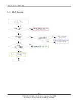
Page 21: ...hooting 9 15 9 9 GSM850 Receiver RX ON Cell Power 60dBm PAM100 Pin15 65dBm Yes Resolder PAM100 C152 C151 L109 L114 C117 No Yes No Check PAM100 Pin9 Pin10 L PAM100 Pin18 68dBm Check ANT Switch control circuit No Yes Resolder PAM100 Yes F101 Pin 8 70dBm Pin 9 70dBm Resolder F101 L119 C119 No Yes Resolder L113 L115 L116 L117 Check UCP200 END ...

Page 22: ...rization 9 16 9 10 GSM Receiver PAM100 Pin15 65dBm Yes Resolder PAM100 C152 C151 L109 L114 C117 No Yes No Check PAM100 Pin9 Pin10 L PAM100 Pin18 68dBm Check ANT Switch control circuit No Yes Resolder PAM100 Yes F101 Pin 6 70dBm Pin 7 70dBm Resolder F101 L119 C119 No Yes Resolder L118 L120 L121 L122 Check UCP200 END RX ON Cell Power 60dBm ...

Page 23: ...hooting 9 17 9 11 DCS Receiver Yes No Resolder F100 C118 L112 F100 Pin 8 70dBm Pin 9 70dBm Yes Resolder PAM100 Yes No Check ANT Switch control circuit Check PAM100 Pin9 H Pin10 L No Yes No Resolder PAM100 C152 C151 L109 L114 C117 Yes PAM100 Pin15 65dBm RX ON Cell Power 60dBm PAM100 Pin17 68dBm Resolder L107 L108 L110 L111 Check UCP200 END ...

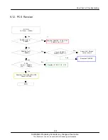
Page 24: ...ization 9 18 9 12 PCS Receiver Yes PAM100 Pin15 65dBm Resolder PAM100 C152 C151 L109 L114 C117 No Yes Check ANT Switch control circuit PAM100 Pin17 68dBm Check PAM100 Pin9 H Pin10 L No No Resolder PAM100 Yes F100 Pin 6 70dBm Pin 7 70dBm Yes No Resolder F100 C118 L112 Resolder L103 L104 L105 L106 Check UCP200 END RX ON Cell Power 60dBm Yes ...

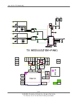
Page 25: ...MP 7 L106 NC 16 19 NC 2 RFIN_HB 4 RFIN_LB RX0 18 RX1 17 8 TX_EN VBATT 11 GND 3 GND 5 6 GND 13 GND GND 20 GPCTRL0 9 10 GPCTRL1 NC 12 PAM100 ANT 15 GND 1 GND 21 22 GND GND 23 24 GND GND 14 L118 R106 L114 L122 3 G G 4 G 5 G 10 1 UNBAL L107 F100 9 BAL1 BAL1 8 7 BAL2 BAL2 6 G 2 L116 C111 L121 C113 L111 GSM900RX_B GSM900RX_A GSM850RX_B GSM850RX_A DCSRX_A DCSRX_B PCSRX_A PCSRX_B VBAT TX_EN PA_HB PA_LB AU...

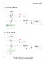
Page 26: ...M100 Yes PAM100 Pin4 65dBm TX ON 5Level Check PAM100 Pin8 H Pin9 L Pin10 H PAM100 Pin15 30dBm Check ANT Switch control circuit Yes Yes Yes No No No END Change or Resolder PAM100 Yes PAM100 Pin4 65dBm TX ON 5Level Check PAM100 Pin8 H Pin9 L Pin10 H PAM100 Pin15 30dBm Check ANT Switch control circuit Yes Yes Yes No No No Resolder R107 END Resolder L109 L114 C117 C151 C152 Resolder L109 L114 C117 C15...

Page 27: ...00 Pin31 65dBm No Resolder R106 Yes Check ANT Switch control circuit PAM pin14 30dBm Check PAM100 Pin8 H Pin9 H Pin10 H No No Change or Resolder PAM100 Yes Yes END TX ON 5Level Yes PAM100 Pin31 65dBm No Yes Check ANT Switch control circuit PAM pin14 30dBm Check PAM100 Pin8 H Pin9 H Pin10 H No No Change or Resolder PAM100 Yes Yes END Resolder L109 L114 C117 C151 C152 Resolder R106 Resolder L109 L11...

Page 28: ...MP 7 L106 NC 16 19 NC 2 RFIN_HB 4 RFIN_LB RX0 18 RX1 17 8 TX_EN VBATT 11 GND 3 GND 5 6 GND 13 GND GND 20 GPCTRL0 9 10 GPCTRL1 NC 12 PAM100 ANT 15 GND 1 GND 21 22 GND GND 23 24 GND GND 14 L118 R106 L114 L122 3 G G 4 G 5 G 10 1 UNBAL L107 F100 9 BAL1 BAL1 8 7 BAL2 BAL2 6 G 2 L116 C111 L121 C113 L111 GSM900RX_B GSM900RX_A GSM850RX_B GSM850RX_A DCSRX_A DCSRX_B PCSRX_A PCSRX_B VBAT TX_EN PA_HB PA_LB AU...

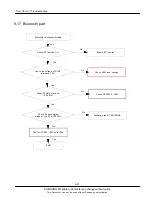
Page 29: ...ting 9 23 9 17 Bluetooth part Bluetooth connection disable Yes Check BT function ON Enable BT function No Yes Check the voltage of R108 is around 3 0V No Check U304 and change Check 26MHz Clock on U106 H6 Yes Check OSC200 U202 No Yes Check the assembled status of the BT ANTENNA No Yes Check UCP200 U106 and U102 Yes END Exchange the BT ANTENNA ...

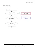
Page 30: ...f Troubleshooting This Document can not be used without Samsung s authorization 9 24 9 18 Radio part Radio does not work Yes Check PMU part No R108 3 0V Yes C144 L126 is OK When U106 operate No Resolder C144 L126 and check U106 Yes Check signal related to U106 Yes END ...

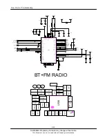
Page 31: ...D C1 VSS C2 UART_CTS_N C3 VSS C4 TM2 C5 SPARE A6 SPARE A7 FM_RXP A8 UART_RTS_N B1 GPIO5 B2 FM_AOUT_L B3 FM_AOUT_R B4 SPARE B5 NC 1 NC 2 GPIO6 FM_IRQ A1 TCXO_MODE A2 SPARE A3 SPARE A4 FM_VDDAUDIO A5 U106 TP113 3 0V_DIG_BT 3 0V_DIG TP109 C150 L123 C129 C141 R112 TP110 3 0V_DIG_BT L126 R113 TP114 TP112 3 0V_DIG_BT C132 TP115 C145 TP107 V_BT_1 2V C133 C144 C127 L124 C131 TP108 V_BT_1 2V V_BT_1 2V C128...

Page 32: ...ion 9 26 9 19 Wi Fi part Wi Fi connection disable Yes Check Wi Fi function ON Enable Wi Fi function No Yes Check the voltage of R101 3 4V R100 3V No Check U304 and change Check 26MHz Clock on U106 H6 Yes Check OSC100 C123 No Yes Check the assembled status of the Wi Fi ANTENNA No Yes Check UCP200 U101 and U102 Yes END Exchange the Wi Fi ANTENNA ...

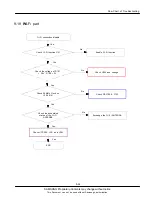
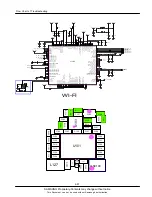
Page 33: ...2 G2 WRF_AFE_PAD_AVDD_RXADC G3 WRF_AFE_PAD_AVDD_AUX G4 WRF_BBPLL_GND_1P2 G5 GMODE_EXT_LNA_PU GMODE_EXT_LNA_GAIN G6 G7 RF_SW_CTRL_N_0 G8 RF_SW_CTRL_P_0 F4 WRF_GPIO_OUT1 F5 VSS F6 VDDIO F7 VDD F8 SDIO_DATA_3 WRF_EXTREFIN F9 G1 WRF_AFE_PAD_AVSS_RXADC G10 VDDIO_SD E6 WRF_VDDVCO_1P2 E7 WRF_GNDVCO_1P2 E8 WRF_VDDCAB_1P2 F1 WRF_AFE_PAD_TEST_IP F10 EXT_POR_L GPIO_9 F11 F2 WRF_AFE_PAD_TEST_IN F3 WRF_AFE_PAD...

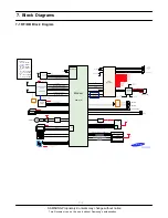
Page 34: ...DET DP DM DP DM UARTA_RXD UARTA_TXD SCL SDA USB_INT BCM21331 3 5PI HEADSET 13X18 ENCLOSURE TYPE MEMORY K522H1HACC 1Gb DDRAM 2Gb NAND DA 0 13 DDQ 0 15 FADQ 0 15 1 8V_MEMORY DBA0 DBA1 DCKE DCLK NAND_ALE NAND_CLE NR DY NANDCEN OEN WEN FWP SIM Socket NC7WZ86L8X MOT_FREQ MOT_INVERT MOT_PDM 3 2V_VIB TOUCH_SDA TOUCH_SCL TOUCH_INT TOUCH_RST MIC2844 LCD_BL_EN LED1 LED2 LED3 LED4 LED5 LED6 VOUT LCD B L Driv...

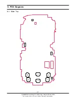
Page 35: ...y Contents may change without notice 8 PCB Diagrams 8 1 This Document can not be used without Samsung s authorization 8 1 Main Top D N E F F 0 0 5 C P F 1 0 5 C P F OK PLAY PAUSE D A P _ V C R W E R D N E S D A P _ K P S ...

Page 36: ...5 F 2 0 5 F GND 0 0 4 A E H 1 0 5 A E H HEA504 0 0 4 C F I L100 L101 L102 3 0 1 L 4 0 1 L 6 0 1 L 5 0 1 L 7 0 1 L L108 L109 L110 1 1 1 L 2 1 1 L 3 1 1 L L114 5 1 1 L 6 1 1 L 7 1 1 L 8 1 1 L L119 0 2 1 L 2 2 1 L 1 2 1 L L123 4 2 1 L L125 L126 L127 L128 9 2 1 L 1 0 2 L 0 0 2 L L202 0 0 3 L 1 0 3 L L400 L401 L402 L403 4 0 4 L 5 0 4 L 6 0 4 L 7 0 4 L 8 0 4 L 9 0 4 L L410 0 0 5 L L501 L502 L503 L504 MI...

Page 37: ...ion Caution 1 Be care of scratch and molding damage Caution 1 Be care of scratch and molding damage Caution 1 Be care of damage to INTENNA Caution 1 Be care of scratch and molding damage 11 1 Disassembly Instructions 1 Unscrew the 6 points 1 1 Unscrew the 2 points 2 3 4 1 Seperate the REAR CASE 1 Separate the LCD and TSP CONNECTORS then disassemble the 2 hook ...

Page 38: ...atch and molding damage Caution 1 Be care of scratch and molding damage 2 Be care of damage to the LCD Caution 1 Be care of damage to FPCB Caution 5 6 7 8 1 Separate the BRACKET ASS Y from the FRONT ASS Y 1 Separate LCD and KEYPAD from the FRONT CASE 1 Detach the SIDE KEY and CAM KEY FPCB from BRACKET 2 Unscrew the 2 points 1 Separate the MOTOR SHIELD CAN INTENNA CAMERA from the PBA ...

Page 39: ...rization Caution 1 Be care of damage the FPCB Caution 1 Be care of damage the RECEIVER FPCB SPK WIRE Caution 1 Be care of damage to INTENNA PATTERN and PBA Caution 1 Be care of damage to PBA 11 2 Assembly instructions 1 2 3 4 1 Solder the SIDE KEY CAM KEY 1 Solder the RECEIVER and SPEAKER 1 Assemble the SPEAKER MODULE to PBA 1 Assemble the SHIELD CAN ...

Page 40: ...zation Caution Caution 1 Be care of damage the MOTOR WIRE Caution 1 Be care of damage to CAMERA CONNECTOR FPCB Caution 1 Be care of damage the SIDE KEY CAMERA KEY FPCB 5 6 7 8 1 Solder the MOTOR 1 Assemble the CAMERA CARRIER 2 Assemble the MOTOR 1 Assemble the CAMERA and connect the CONNECTOR 1 Assemble the BRACKET 2 Attach the SIDE KEY and CAM KEY FPCB ...

Page 41: ...f scratch and molding damage 2 Be care of damage to TSP FPCB Caution 1 Be care of damage to F CPB and LCD 2 Be care of scratch and molding damage Caution 1 Be care of damage to F CPB 2 Be care of scratch and molding damage 9 10 11 12 1 Screw 2 points 1 Attach the TSP 2 Assemble the KEYPAD 1 Assemble the LCD 1 Assemble the PBA the to FRONT ASS Y 2 Connect the TSP connector LCD connector ...

Page 42: ...ment can not be used without Samsung s authorization Caution 1 Be care of scratch and molding damage Caution 1 Be care of scratch and molding damage Torque 1 0 1 2 Kgf cm Caution 1 Be care of scratch and molding damage Torque 1 0 1 2 Kgf cm 13 14 1 Screw 2 points 1 Assemble the REAR CASE 15 1 Screw 6 points ...

Reviews: