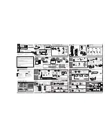
2. Out put Bl ock
DVD- HR755 has four stereo analog line out terminal, and two digital output
terminal.
Decoded signal by DIC1 is inputted to VIC1( D/A converter), then filtered and
amplified by IC217(OP- amp),and finally ouputted via AV switch IC(IC216).
The Signal outputted via AV2 is equal to those of AV1(Scart), and RCA Analog ouput
terminal in normal mode.
The Digital audio signal is drived by AIC3 inverter and ouputted via Optical(TOS- link)
and Coaxial(S/PDIF) terminal.
switchig IC) - >VIC1(A/D coverter) - >
DIC1(MPEG Encorder/Decoder)
So audio signal flows like this : AV input Jack - > IC216(Mux switchig IC)
- - >VIC1(A/D coverter) - > DIC1(MPEG Encoder/Decorder)- >Digital ouput or
VIC1(DAC) - > IC216((Mux switchig) - > AV output Jack
1. I nput bl ock
DVD- HR755 has three stereo line input terminals(AV1,AV2,AV3) and internal TV- audio
from RF Tuner Block.
These four analog audio signal source are selected in IC216.
The switching operation of IC216 is controlled by FIC1(Front Micom) with I2C
interface. This analog audio signal is convereted to by AD convert. VICA is
syncronized by three Digital clock from DIC1, and output Digital signal
Summary of Contents for DVD-HR750
Page 11: ...1 Top Cabi net Rem oval...
Page 12: ...2 As s y Fr ont Cabi net Rem oval...
Page 13: ...3 Har d Di s k Rem oval...
Page 14: ...4 As s y Deck Rem oval...
Page 15: ...5 Mai n PCB and S M P S PCB Rem oval...
Page 16: ...6 Jack PCB Rem oval...
Page 17: ...7 DC FAN Rem oval...
Page 18: ...Description Front Panel...
Page 19: ...Description Rear Panel...
Page 20: ...Description Front Panel Display...
Page 21: ...Supplide Accessary DVD HR755 supply below accessary...
Page 22: ...Product Specifications European model...
Page 23: ...Product Specifications Asia and Australia model...
Page 24: ...Chassis Product Specifications European model...
Page 25: ......
Page 26: ......
Page 27: ...Chassis Product Specifications Asia and Australia model...
Page 28: ......
Page 29: ......
Page 31: ...1 Overall block diagram Block Diagram...
Page 32: ...2 Wiring diagram MAI N PCB Wiring Diagram...
Page 35: ...5 Vi deo I nt er f ace...
Page 42: ...10 AUDI O...
Page 44: ...11 Ci r cui t Di agr am Circuit Diagram...
Page 46: ...MTS s i gnal t abl e...
Page 48: ...13 Tuner Dem odul at or Bl ock di agr am of Tuner...
Page 56: ...16 Tr oubl es hoot i ng For s er vi ce engi neer...
Page 57: ......
Page 58: ......
Page 59: ......
Page 60: ......
Page 61: ......
Page 62: ......
Page 63: ......
Page 64: ......
Page 65: ......
Page 66: ......
Page 67: ......
Page 68: ......
Page 69: ......


