
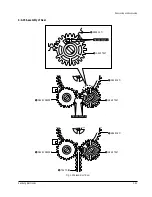


Circuit Descriptions
5-12
Samsung Electronics
5-4-3 Operation
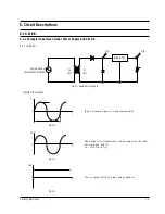
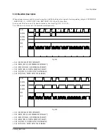
1) FOCUSING SERVO
(1) FOCUS INPUT
The focus loop is changed from open loop to closed loop, and the triangular waveform moves the object lens up
and down (at pin 75 of SIC1 during Focus SERVO ON.) At that time, S curve is input to pin 65 of SIC1.
ABAD (pin 39 of RIC1) signal, summing signal of PD A, B, C, D, is generated, and zero cross(2.5V) point occurs
when S curve is focused and ABAD signal exceeds a preset,constant value. The focus loop is changed to
closed loop, and the object lens follows the disc movement, maintaining a constant distance from the disc.
(these operations are same in CD and DVD).
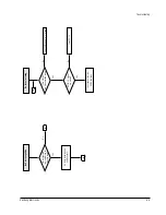
Fig. 5-18
Vref
Vref
1.5V
Pin75 of SIC1 (FOD)
Pin65 of SIC1 (FEI)
Pin39 of RIC1 (ABCD)
(2) PLAY
When focus loop closes the loop during focus servo on, both pin 65 and pin 75 of SIC1 are controlled by VREF
voltage (approx. 2.5V), and pin 1, 2 of DRIC2 are approximately 4.5V.
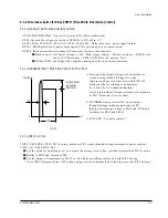
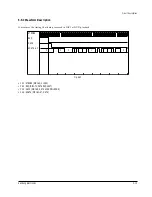
2) TRACKING SERVO
(1) NORMAL PLAY MODE
Œ
For DVD
Composite : The signal output from PD A, B, C, D of Pick-up, the tracking error signal (pin36 of RIC1) uses the
phase difference of A+C and B+D in RIC1, and inputs to terminal 64 of SIC1. Then, it is output to SIC1 pin 76 via
digital equalizer, and applied to the tracking actuator through DRIC2.
Pins 17, 18 of SIC1 are controlled by VREF(approx. 2.5V) during normal play.
Meanwhile, DVD repeats the track jump from 1 to 4 in inner direction at normal play (because data- read speed
from disc is faster than data output speed on screen).
´
For CD, VCD
Receive the signal output through E, F of Pick-up, from RIC1. The tracking error signal is similar to DVD.
Summary of Contents for DVD-C600
Page 23: ...Reference Information 2 16 Samsung Electronics MEMO ...
Page 49: ...4 24 Samsung Electronics Disassembly and Reaasembly MEMO ...
Page 79: ...Troubleshooting 6 10 Samsung Electronics MEMO ...
Page 85: ...Exploded Views and Parts List 7 6 Samsung Electronics MEMO ...
Page 91: ...8 6 Samsung Electronics Electrical Parts List MEMO ...
Page 95: ...PCB Diagrams 10 2 Samsung Electronics 10 1 Main COMPONENT SIDE SOLDER SIDE ...
Page 96: ...PCB Diagrams Samsung Electronics 10 3 10 2 Jack ...
Page 97: ...PCB Diagrams 10 4 Samsung Electronics 10 3 S M P S ...
Page 98: ...PCB Diagrams Samsung Electronics 10 5 10 4 Front COMPONENT SIDE SOLDER SIDE ...
Page 99: ...PCB Diagrams 10 6 Samsung Electronics 10 5 Key COMPONENT SIDE SOLDER SIDE ...
Page 100: ...PCB Diagrams Samsung Electronics 10 7 10 6 Head Phone 10 7 Deck COMPONENT SIDE SOLDER SIDE ...
Page 101: ...PCB Diagrams 10 8 Samsung Electronics 10 8 Sensor 10 9 Motor ...
Page 103: ...Wiring Diagram 11 2 Samsung Electronics MEMO ...
Page 105: ...Schematic Diagrams 12 2 Samsung Electronics 12 1 S M P S ...
Page 106: ...Schematic Diagrams Samsung Electronics 12 3 12 2 Main Power Supply ...
Page 107: ...Schematic Diagrams 12 4 Samsung Electronics 12 3 Main Micom ...
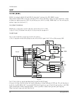
Page 108: ...Schematic Diagrams Samsung Electronics 12 5 12 4 Servo ...
Page 109: ...Schematic Diagrams 12 6 Samsung Electronics 12 5 Video Encoder ...
Page 110: ...Schematic Diagrams Samsung Electronics 12 7 12 6 Video CVBS Output Y Output C Output ...
Page 111: ...Schematic Diagrams 12 8 Samsung Electronics 12 7 Audio DAC ...
Page 112: ...Schematic Diagrams Samsung Electronics 12 9 12 8 Audio ...
Page 113: ...Schematic Diagrams 12 10 Samsung Electronics 12 9 RF ...
Page 114: ...Schematic Diagrams Samsung Electronics 12 11 12 10 ZiVA ...
Page 115: ...Schematic Diagrams 12 12 Samsung Electronics 12 11 DSP ...
Page 116: ...Schematic Diagrams Samsung Electronics 12 13 12 12 Front Micom VFD Display ...
Page 118: ...Schematic Diagrams Samsung Electronics 12 15 12 14 Head Phone ...
Page 119: ...Schematic Diagrams 12 16 Samsung Electronics 12 15 Key ...
Page 120: ...Schematic Diagrams Samsung Electronics 12 17 12 16 Deck ...
Page 121: ...Schematic Diagrams 12 18 Samsung Electronics 12 17 Deck Control ...
Page 122: ...Schematic Diagrams Samsung Electronics 12 19 12 18 Remote Control ...
Page 123: ...Schematic Diagrams 12 20 Samsung Electronics MEMO ...