
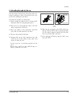


Reference Information
Samsung Electronics
2-3
17
16
15
14
13
12
11
10
9
8
7
6
5
4
3
2
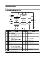
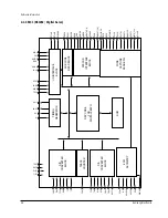
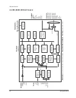
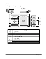
CD optical main beam A AC coupling input port for RF
CD optical main beam B AC coupling input port for RF
CD optical main beam C AC coupling input port for RF
CD optical main beam D AC coupling input port for RF
DVD optical main beam A AC coupling input port for RF
DVD optical main beam B AC coupling input port for RF
DVD optical main beam C AC coupling input port for RF
DVD optical main beam D AC coupling input port for RF
RF AMP I/O buffer bias resistance connection port
RF EQ bias resistance connection port
Analog block bias resistance connection port
CAP connection port for RF EQ center voltage
CD optical sub beam E input port for SERVO
CD optical sub beam F input port for SERVO
DVD optical main beam A input port for SERVO
DVD optical main beam B input port for SERVO
DVD optical main beam C input port for SERVO
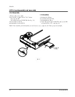
1
ACD
BCD
CCD
DCD
ADVD
BDVD
CDVD
DDVD
RREFBF
RREFEQ
RREF
VREFEQ
E
F
ADVD1
BDVD1
CDVD1
FUNCTION
PIN NAME
I/O
I
I
I
I
I
I
I
I
-
-
O
I
I
I
I
I
-
38
37
36
35
34
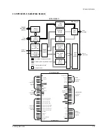
FE Input port for AMP GAIN setting
Input port for TE AMP GAIN setting
TE AMP output port
Bias resistance port for PDLIMIT
Input port for ABCD AMP GAIN setting
FEN
TEN
TE
PDLIMTRES
ABCDN
FUNCTION
PIN NAME
I/O
I
I
O
-
I
28
27
26
25
24
23
22
21
20
19
DVD optical main beam D input port for SERVO
CD optical main beam F input port for SERVO
CD optical main beam F input port for SERVO
CD optical main beam F input port for SERVO
CD optical main beam F input port for SERVO
Power voltage input port for analog part
CAP connection port for analog part
center voltage, Use at other block
CAP connection port for focus auto offset (OPEN)
ON/OFF connection port for auto offset block (L :
auto offset adjustment H : serial offset adjustment)
BANDGAP voltage input port for ALPC
DVD optical laser diode driving voltage output port
18
DDVD1
ACD1
BCD1
CCD1
DCD1
AVCC
VREF
A
FOFST
OFSTHOLD
VREFLP_BGI
LDODVD
I
I
I
I
I
-/O
O
I
O
I
P
32
31
30
29
DVD optical laser monitor diode voltage input port
CD optical laser diode driving voltage output port
CD optical laser monitor diode voltage input port
Power GND port for analog part
PDDVD
LDOCD
PDCD
AGND
I
O
I
P
33
FE AMP output port
FE
O
ABCD AC coupling input port for SERVO monitor
ABCDI
I
48
47
46
45
44
43
42
41
40
ABCD AMP output port
Peak hold time constant setting RC
connection port for RF envelope detect
Bottom hold time constant setting RC
connection port for RF envelope detect
RF envelope detect output port
Power GND input port for digital circuit
Focus OK comparing level input port
Focus OK comparator output port
(L: FOCUS OK)
Peak hold time constant connection port SERVO
defect max. time setting
Peak hold time constant connection port PLL defect
min. time setting
39
ABCD
ENVP
ENVB
ENV
DGND
FOKTH
FOKB
DFCT_CP1
DFCT_CP2
O
-
-
O
I
O
-
-
P
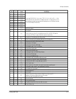
62
61
60
59
58
57
56
55
54
53
52
51
50
49
Output port of peak detector for defect
AC coupling input port for defect
Power voltage input port for digital circuit
Resistance connection port for PLL defect comparat-
ing level setting
Resistance connection port for SERVO defect com-
parating level setting
Defect output port for SERVO
Defect output port for PLL
Power voltage input port for DPD TE
Mirror output port
BCA output port
Resistance connection port for 3BTE offset
DPD EQ (A+C) output port
DPD EQ (B+D) output port
DPD defect waveform output port (MONITOR)
CC1
CC2
DVCC
DVCTTH2
DFCTTH1
DFCT1
DFCT2
DPDVCC
MIRR
BCA
TE3OFST
DPDEQ1
DPDEQ2
FAUL
TOUT
O
P
-
-
I
O
O
P
O
O
-
O
O
O
64
DPD TE MUTE control port (H : MUTE)
DPD TE PLL variable input port
63
DPDMUTE
PLLCTL
I
I
FUNCTION
PIN NAME
I/O
FUNCTION
PIN NAME
I/O
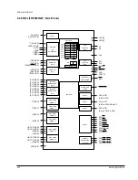
87
86
85
84
83
82
81
80
79
78
77
76
75
74
73
72
71
70
69
68
67
66
65
DPD TE PLL variable bias resistance
Power GND input port for DPD TE
CAP connection port for DPD TE center
Bias resistance connection port for delta block
Data input port
Clock input port
Data enable input port
OSC time constant input port for auto offset block
Reset input port for auto offset block (L : RESET)
BCA FIL
TER1
BCA FIL
TER2
RF ripple center voltage output port for mirror
Bottom hold time constant RC connection port for
RFCT generation
Peak hold time constant RC connection port for
RFCT generation
RF ripple AMP output port for mirror
RF ripple AMP GAIN input port for mirror
RF ripple offset control port for mirror
Bottom hold time constant RC connection port for
RFCT generation
Peak hold time constant RC connection port for
RFCT generation
Input port for MIRR signal generation
Power voltage input port for RF EQ
RF EQ output port
BCA comparating level control port
TE1RES
DPDGND
VREFDPD
RREFDL
Y
DA
TA
CLOCK
STB
OSC
RESET
BCAI
BCAO
RFCT
CB2
CP2
RFRP
RFRPN
MROFST
CB1
CP1
MIRRI
EQVCC
RFEQO
BCA
TH
I
P
O
-
I
I
I
I
I
O
O
-
-
O
I
I
-
-
I
P
O
I
91
90
89
RF
AGCO input port for RF EQ
RF AGC AMP output port
AGC time constant CAP connection port
When AGC is “HOLD”, AGC voltage input port
88
EQIN
RF
AGCO
AGCC
AGCI
I
O
-
I
95
94
93
92
Power GND input port for RF EQ
AGC level control voltage input port
RF bottom hold time constant RC connection por
t for RF AGC
RF peak hold time constant RC connection por
t for RF AGC
EQGND
AGCLEVEL
AGCB
AGCP
P
I
-
-
100
99
98
97
96
Bias resistance connection port for RF EQ frequency setting
RF EQ boost gain control voltage input port
RF EQ peak frequency control voltage input port
RF EQ boost, peak frequency gain control port corre-
sponding to wideband PLL (PLLG. PLLF resistance
internal design)
RF EQ control port (When No. PLLG isn’
t adjusted,
apply DC CTL voltage.)
RDPF
EQG
EQF
PLLGF
VZOCTL
-
I
I
I
I
Summary of Contents for DVD-C600
Page 23: ...Reference Information 2 16 Samsung Electronics MEMO ...
Page 49: ...4 24 Samsung Electronics Disassembly and Reaasembly MEMO ...
Page 79: ...Troubleshooting 6 10 Samsung Electronics MEMO ...
Page 85: ...Exploded Views and Parts List 7 6 Samsung Electronics MEMO ...
Page 91: ...8 6 Samsung Electronics Electrical Parts List MEMO ...
Page 95: ...PCB Diagrams 10 2 Samsung Electronics 10 1 Main COMPONENT SIDE SOLDER SIDE ...
Page 96: ...PCB Diagrams Samsung Electronics 10 3 10 2 Jack ...
Page 97: ...PCB Diagrams 10 4 Samsung Electronics 10 3 S M P S ...
Page 98: ...PCB Diagrams Samsung Electronics 10 5 10 4 Front COMPONENT SIDE SOLDER SIDE ...
Page 99: ...PCB Diagrams 10 6 Samsung Electronics 10 5 Key COMPONENT SIDE SOLDER SIDE ...
Page 100: ...PCB Diagrams Samsung Electronics 10 7 10 6 Head Phone 10 7 Deck COMPONENT SIDE SOLDER SIDE ...
Page 101: ...PCB Diagrams 10 8 Samsung Electronics 10 8 Sensor 10 9 Motor ...
Page 103: ...Wiring Diagram 11 2 Samsung Electronics MEMO ...
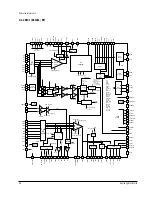
Page 105: ...Schematic Diagrams 12 2 Samsung Electronics 12 1 S M P S ...
Page 106: ...Schematic Diagrams Samsung Electronics 12 3 12 2 Main Power Supply ...
Page 107: ...Schematic Diagrams 12 4 Samsung Electronics 12 3 Main Micom ...
Page 108: ...Schematic Diagrams Samsung Electronics 12 5 12 4 Servo ...
Page 109: ...Schematic Diagrams 12 6 Samsung Electronics 12 5 Video Encoder ...
Page 110: ...Schematic Diagrams Samsung Electronics 12 7 12 6 Video CVBS Output Y Output C Output ...
Page 111: ...Schematic Diagrams 12 8 Samsung Electronics 12 7 Audio DAC ...
Page 112: ...Schematic Diagrams Samsung Electronics 12 9 12 8 Audio ...
Page 113: ...Schematic Diagrams 12 10 Samsung Electronics 12 9 RF ...
Page 114: ...Schematic Diagrams Samsung Electronics 12 11 12 10 ZiVA ...
Page 115: ...Schematic Diagrams 12 12 Samsung Electronics 12 11 DSP ...
Page 116: ...Schematic Diagrams Samsung Electronics 12 13 12 12 Front Micom VFD Display ...
Page 118: ...Schematic Diagrams Samsung Electronics 12 15 12 14 Head Phone ...
Page 119: ...Schematic Diagrams 12 16 Samsung Electronics 12 15 Key ...
Page 120: ...Schematic Diagrams Samsung Electronics 12 17 12 16 Deck ...
Page 121: ...Schematic Diagrams 12 18 Samsung Electronics 12 17 Deck Control ...
Page 122: ...Schematic Diagrams Samsung Electronics 12 19 12 18 Remote Control ...
Page 123: ...Schematic Diagrams 12 20 Samsung Electronics MEMO ...