background image

Circuit Description

Samsung Electronics

13-3

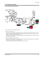
13-2 Partial Block Description

13-2-1 Vertical & N/S Correction Circuit

Understanding of N/S Circuit and Operation Principle. 

What is a N/S correction circuit?

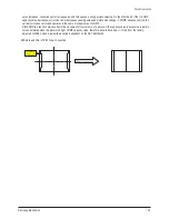
- If the bias angle of a picture widens, the distance from the center of a picture to each corner becomes farther as it moves to

periphery. This causes the picture being distorted (Picture Lowering) vertically in a shape of a spool because of the strong 
bias at four corners which are the farthest from the center. 

Correction effect to the amount of a correction signal can be made by crossing Parabolic current of a vertical period over the 

vertical bias current and applying it.

N/S Circuit Constitution and Operation Principle.

- Consists of L304, C305, C439, R312. Symmetrize the up and down amplitude using the saturable reactor of L304 and adjust 

N/S Gain by controlling the capacity value of C305 and C439
If the correction vector is excessive, one can slightly reduce the resistance of R312

Summary of Contents for CS29Z30SPBXBWT

Page 1: ...COLOR TELEVISION RECEIVER Chassis S62B P _Corset Model CS29Z30SPBXBWT COLOR TELEVISION RECEIVER FEATURES Slimfit Low Depth CRT SRS WOW Simple 100Hz SERVICE Manual CS 29Z30SPQ...

Page 2: ...is a property of Samsung Electronics Co Ltd Any unauthorized use of Manual can be punished under applicable International and or domestic law Samsung Electronics Co Ltd Sep 2005 Printed in Korea AA82...

Page 3: ...ccess Service Mode 3 2 3 3 Factory Data 3 3 3 4 Service Adjustment 3 24 3 5 Replacements Calibration 3 26 Chapter 4 Exploded View Part List 4 1 CS29Z30SPBXBWT 4 1 Chapter 5 Electrical Part List 5 1 CS...

Page 4: ...10 9 10 5 AV 10 10 10 6 CONTROL 10 11 10 7 LED Module 10 12 10 8 Master S W 10 12 Chapter 11 Operation Instruction Installation 11 1 Product Features and Functions 11 1 Chapter 12 Disassembly Reassemb...

Page 5: ...ut insulated transistors the product can only be repaired safely when the chassis is connected to the earthed end of the AC power source To make sure the AC power cord is properly connected follow the...

Page 6: ...placed with another irregular one the safety or protective features will be lost even if the new one has a higher voltage or more watts Critical safety parts should be bracketed with Use only regular...

Page 7: ...c 6 Insulation Check Process Unplug the power cord from the AC source and turn the switch on Connect the insu lating resistance meter 500v to the AC plug blade The insulating resistance between the bl...

Page 8: ...for soldering purposes 6 Use only anti static solder removal devices Most solder removal devices do not support an anti static feature A solder removal device without an anti static feature can store...

Page 9: ...being exposed to moisture Otherwise it may cause a fire or electric shock 5 Make sure to turn the power off and unplug the power cord from the outlet before removing the product Also check the antenna...

Page 10: ...1 6 Samsung Electronics MEMO...

Page 11: ...A2165 Audio Output 10W x 2 Function A2 Nicam SRS WOW STV8237 STV8237 Cabinet New Front and Back Cabinets 184mm of saved space compared to the existing model A11 580mm Z30 396mm Z30 OZ Design Applied F...

Page 12: ...lti System PAL SECAM CIS Option NTSC4 43 NTSC3 58 ATS Auto Wide Pre Channel On Off Timer Zoom Blue Screen Picture System Video PAL SECAM NTSC3 58 CIS Option Sound B G D K I L L M CIS Option Black Leve...

Page 13: ...O O O DNIe 3 2 Pull Down Support Audio Base Treble Balance Equalizer 5 Band 5 Band 5 Band AVL O O O Surround Virtual Dolby Virtual Dolby SRS WOW Speaker System SEMI DOME SEMI DOME Direct Speaker Outp...

Page 14: ...01 000121 Samsung Service center Owner s Instructions Safety Guide Manual AA68 03635F AA68 03242E Warranty Card Registration Card AA68 03278B AA68 03576A Accessories that can be purchased additionally...

Page 15: ...odel Some of the contents may be changed subject to the sales location and the product specifications 2 When replacing the F_Box Board Since the software is loaded to the EPROM of the F_box board chec...

Page 16: ...cedure above 2 The initial screen of Service Mode Europe Asia CIS 3 Functions of the Keys within Service Mode Service T_SHPEU_XXXX Option XX XX XX Deflection Video Adjust 1 Video Adjust 2 Video Adjust...

Page 17: ...0 34 Adjust 10 Lower Corner 39 37 Adjust 11 H Trapezium 26 28 Adjust 12 Bow 33 34 Fix 13 Angle 32 34 Fix 14 V Position 40 40 Fix 1 Deflection Adiustment PAL No item WS32Z306VB CW29Z306VB Remark Data D...

Page 18: ...Alignment Adjustment 3 4 Samsung Electronics...

Page 19: ...1 H Shift_NTSC 0 0 Adjust 3 4 3 Offset__Vixlim No item WS32Z306VB CW29Z306VB Remark Data Data 0 EE_R_CUTOFF 32 32 Adjust 1 EE_G_CUTOFF 32 32 Fix 2 EE_B_CUTOFF 32 32 Adjust 3 Color On Off 1 1 Adjust 4...

Page 20: ...pass_AV 6 6 Fix 18 Highpass_AV 7 7 Fix 19 Nicam MAE value 255 255 Fix 5 Video Adjustment 2 No item WS32Z306VB CW29Z306VB Remark Data Data 0 H_EHT comp 4 0 Fix 1 V_EHT comp 5 4 Fix 2 PIN EHT comp 6 5 F...

Page 21: ...6VB Remark Data Data 0 R_Drive Warm2 3 3 Fix 1 B_Drive Warm2 9 9 Fix 2 R_Cutoff_Warm2 6 6 Fix 3 B_Cutoff_Warm2 11 11 Fix 4 R_Drive Warm1 2 2 Fix 5 B_Drive Warm1 2 2 Fix 6 R_Cutoff_Warm1 3 3 Fix 7 B_Cu...

Page 22: ...ix 1 System VGA 2 2 2 System 480p 2 2 Fix 3 System 1080i 3 3 Fix 4 Dynamic Contrast 90 90 Fix 5 Dynamic Brightness 50 50 Fix 6 Dynamic Shapness 50 50 Fix 7 Dynamic Color 50 50 Fix 8 Dynamic Tint 50 50...

Page 23: ...19 Fix 44 LTI Mode 2 1 1 Fix 45 LTI Mode VGA 46 LTI Mode 480p 1 1 Fix 47 LTI Mode 1080i 1 1 Fix 48 NR ON value1 85 85 Fix 49 NR ON value2 85 85 Fix 50 NR OFF value1 68 68 Fix 51 NR OFF value2 68 68 Fi...

Page 24: ...tion 86 3Pip Ntsc H Position 87 88 89 90 RF SubBright 124 124 Fix 91 TTX Sub Brightness 235 235 Fix 92 Left Blanking 101 101 Fix 93 Right Blanking 153 153 Fix 94 S ABL 0 0 Fix 95 P ABL 48 80 Fix 96 Pi...

Page 25: ...e 4 3 depending on the CRT 2 AV_JACK Scart Scart Scart RCA 3 DTV Off Off On Off 4 PIP Off Off 2 Tuner 1 Tuner Off depending on the model 5 LNA Off Off On Off On 2T PIP LNA All model Off 1Tuner No PIP...

Page 26: ...17 Zoom1 Tra offset 4 6 2 Fix 18 Zoom2 Tra offset 7 10 8 Fix 2 Deflection Adiustment NTSC Asia CIS No item CIS 29 CIS 32 Asia 29 Remark Data Data Data 0 V Amp 38 29 39 Adjust 1 V_SHIFT 23 23 23 Adjus...

Page 27: ...232 232 Fix 16 CXA2151 Sub02 97 97 97 Fix 17 Zoom1 Tra offset 0 0 0 Fix 18 Zoom2 Tra offset 0 0 0 Fix 3 576P Deflect Offset No item CIS 29 CIS 32 Asia 29 Remark Data Data Data 0 V Amp 0 0 0 Fix 1 V_S...

Page 28: ...Fix 11 H Shift_NTSC 0 0 0 Adjust 6 4 3 Offset__Vixlim No item CIS 29 CIS 32 Asia 29 Remark Data Data Data 0 V Amp 12 12 11 Fix 1 V_SHIFT 6 6 0 Fix 2 H EW 22 22 22 Fix 3 H Shift 0 0 0 Fix 4 V Linearit...

Page 29: ...Tint 28 28 28 Fix 15 CTI Level 1 1 1 Fix 16 Color AXIS 1 1 1 Fix 17 LTI Mode 1 1 1 Fix 18 LTI Level 3 3 3 Fix 19 VSU 3 5 5 Fix 20 Melody volume 9 9 9 Fix 21 Video mute time 6 6 6 Fix 7 Video Adjustmen...

Page 30: ...Asia 29 Remark Data Data Data 0 H_EHT comp 0 2 0 Fix 1 V_EHT comp 4 5 4 Fix 2 PIN EHT comp 5 6 5 Fix 3 AFC EHT comp 0 0 0 Fix 4 Sync Phase 0 0 0 Fix 5 NR Value 6 6 6 Fix 6 PIP Contrast 14 14 14 Fix 7...

Page 31: ...ol2 0 0 0 Fix 19 B_Cutoff_Cool2 9 9 0 Fix 11 Video Adjustment 5 No item CIS 29 CIS 32 Asia 29 Remark Data Data Data 0 R drive offset 1080i 1 1 1 Fix 1 G drive offset 1080i 5 5 5 Fix 2 R cutoff offset...

Page 32: ...Fix 11 SHP CD 1 1 1 Fix 12 SHP f0 1 1 1 Fix 13 SHP f1 p10 12 12 12 Fix 14 LTI level 2 2 2 Fix 14 DTV Video Adjustment 576p No item CIS 29 CIS 32 Asia 29 Remark Data Data Data 0 Sub Bright 37 37 37 Fix...

Page 33: ...1 1 Fix 12 SHP f0 1 1 1 Fix 13 SHP f1 p10 12 12 12 Fix 14 LTI level 1 1 1 Fix 15 H_EHT comp_1080i 1 1 0 Fix 16 V_EHT comp_1080i 3 3 4 Fix 17 PIN EHT comp_1080i 5 5 5 Fix 18 ABL TH_1080i 3 3 3 Fix 15 D...

Page 34: ...System 1 1 1 Fix 1 System VGA 1 1 1 Fix 2 System 480p 2 2 2 Fix 3 System 1080i 3 3 3 Fix 4 Dynamic Contrast 90 90 100 Fix 5 Dynamic Brightness 50 50 55 Fix 6 Dynamic Shapness 50 50 75 Fix 7 Dynamic Co...

Page 35: ...255 255 255 Fix 44 480i_Sub Bright 44 44 44 Fix 45 480i_Sub Contrast 10 10 10 46 576i_Sub Bright 46 46 46 Fix 47 576i_Sub Contrast 10 10 10 Fix 48 NR ON value1 85 85 85 Fix 49 NR ON value2 85 85 85 Fi...

Page 36: ...15 215 Fix 77 Adjusting Chroma PLL 1 1 1 78 WSS 4 3 Panorama 255 255 255 79 NT left blank 150 150 150 Fix 80 NT Right blank 92 92 92 Fix 81 Progressive TTX V Position 255 255 255 82 Progressive TTX H...

Page 37: ...ed by FBThigh pressure 150 150 150 Fix No Option Byte CIS 29 CIS 32 Asia 29 Middle East 29 Remark Data Data Data Data 1 CRT 4 3 Wide 4 3 4 3 depending on the CRT 2 OSD Group CIS CIS East Asia Arab 3 O...

Page 38: ...Factory Data the picture size has to be adjusted when replacing the System Board or the Deflection Board according to the following procedures Display the Lion pattern Press Info Menu Mute Power On us...

Page 39: ...pattern and check that the picture size has not been changed If there is no change finish the adjustments Adjust BOW and the Angle settings so that the center line becomes a straight line Adjust the H...

Page 40: ...View as Standard 3 Turn the Static Focus VR clockwise to the maximum position End of clockwise direction 4 Turn the Dynamic Focus VR counter clockwise to the maximum position End of counter clockwise...

Page 41: ...the Toshiba pattern 4 Using an Oscilloscope measure the size of RK BK and GK to the Pedestal Level 5 Adjust the Screen VR of FEB so that the highest point of the Pedestal Level is 175V Screen Voltage...

Page 42: ...n changed 8 If you have readjusted Low Light readjust High Light until the two values are identical to the coordinates of the corresponding model White Balance Standard Data 3 5 4 Check List for the S...

Page 43: ...0022 AA64 01201N KNOB CONTROL 32Z30 ABS HB BLK 1 S N A T0023 BP64 00326A KNOB POWER 43T9 ABS HB BLK SVM3012 1 S A T0057 AA64 01062B BADGE BRAND ALL AL T1 5 10 6 L65 BLK SIL 1 S A T0063 AA03 00443A CRT...

Page 44: ...16x25 7 5 1 S A CIS1 0205 001154 OIL SILICON G746 0 S N A CIS1 0205 001154 OIL SILICON G746 0 S N A CIS1 0205 001154 OIL SILICON G746 0 S N A CN301 AA60 40012F PIN GT 4P 2 36PI 6 12 14mm NYLON66 LOCKI...

Page 45: ...00002 EYELET ID1 5 OD2 L2 8 NI SN BSP3 1 2H 1 S N A EY420 6042 000002 EYELET ID1 5 OD2 L2 8 NI SN BSP3 1 2H 1 S N A EY421 6042 000002 EYELET ID1 5 OD2 L2 8 NI SN BSP3 1 2H 1 S N A EY422 6042 000002 EY...

Page 46: ...SY HEAT SINK P AA62 00072C SCREW FJL69 1 S N A Q404 BP96 00020P ASSY HEAT SINK P AA62 00045A SCREW FQP63 1 S N A Q409 0505 001116 FET SILICON BUZ73A N 200V 22A 0 6ohm 40W 1 S A Q409 0505 001723 FET SI...

Page 47: ...93 AA39 00387C LEAD CONNECTOR K62A CORE UL1007 26 4P 7 1 S A PCB AA41 00619A PCB CONTROL Z7 CT 29HM8 FR 1 1L A 1 6T 1 S N A RY02 2001 000577 R CARBON 2KOHM 5 1 8W AA TP 1 8X3 2MM 1 S A RY03 2001 00000...

Page 48: ...Sn 37Pb 0 S N A T0245 AA39 20179A LEAD CONNECTOR ASSY 3 2 P 300MM YFH800 1 S A T0286 AA94 15180A ASSY PCB MISC MASTER S W OZ S62A 1 S A T0523 AA61 00530B BRACKET MASTER 25M6 29M6 SECC 1 S N A AA97 158...

Page 49: ...M LEAD PEF 47nF 5 50V TP 7 5x4 0x6 1 S A C822 2201 000599 C CERAMIC DISC 0 56NF 10 500V Y5P TP 5 1 S A C823 2401 003141 C AL 2200uF 20 25V WT TP 13x25 5mm 1 S A C824 2201 000332 C CERAMIC DISC 2 2nF 2...

Page 50: ...0 400V Y5U TP 9 5X6 1 S A D202 0401 000133 DIODE SWITCHING RLS4148 75V 150MA LL 34 1 S A D401 0401 000005 DIODE SWITCHING 1N4148 75V 150MA DO 35 T 1 S A D402 0401 000005 DIODE SWITCHING 1N4148 75V 150...

Page 51: ...0401 000133 DIODE SWITCHING RLS4148 75V 150MA LL 34 1 S A DD03 0403 001117 DIODE ZENER RLZ12B 11 44 12 03V 500MW LL 1 S A DD04 0403 001117 DIODE ZENER RLZ12B 11 44 12 03V 500MW LL 1 S A DD05 0403 001...

Page 52: ...CHIP 47ohm 5 1 10W TP 1608 1 S A DR43 2007 000078 R CHIP 1Kohm 5 1 10W TP 1608 1 S A DR44 2007 000078 R CHIP 1Kohm 5 1 10W TP 1608 1 S A DR45 2007 000078 R CHIP 1Kohm 5 1 10W TP 1608 1 S A DR46 2007 0...

Page 53: ...10 16V X7R 1608 1 S A EC25 2203 000783 C CER CHIP 0 33nF 5 50V C0G 1608 1 S A EC26 2203 000783 C CER CHIP 0 33nF 5 50V C0G 1608 1 S A EC27 2203 000783 C CER CHIP 0 33nF 5 50V C0G 1608 1 S A EC28 2203...

Page 54: ...10W TP 1608 1 S A ER16 2007 000074 R CHIP 100ohm 5 1 10W TP 1608 1 S A ER19 2007 000074 R CHIP 100ohm 5 1 10W TP 1608 1 S A ER20 2007 000074 R CHIP 100ohm 5 1 10W TP 1608 1 S A ER21 2007 001167 R CHI...

Page 55: ...S N A EY828 6042 000002 EYELET ID1 5 OD2 L2 8 NI SN BSP3 1 2H 1 S N A EY829 6042 000002 EYELET ID1 5 OD2 L2 8 NI SN BSP3 1 2H 1 S N A EY830 6042 000002 EYELET ID1 5 OD2 L2 8 NI SN BSP3 1 2H 1 S N A E...

Page 56: ...N A JA701 3722 001884 JACK SCART 42P SNPB BLK 1 S A L101 2701 000115 INDUCTOR AXIAL 10UH 10 3070 1 S A L102 2701 000159 INDUCTOR AXIAL 22UH 10 4298 1 S A L103 2701 000115 INDUCTOR AXIAL 10UH 10 3070...

Page 57: ...A MC33 2402 000176 C AL SMD 10uF 20 16V GP TP 4 3x4 3x5 4 1 S A MC34 2402 000176 C AL SMD 10uF 20 16V GP TP 4 3x4 3x5 4 1 S A MC35 2402 000176 C AL SMD 10uF 20 16V GP TP 4 3x4 3x5 4 1 S A MC36 2402 00...

Page 58: ...310mW SOT 23 T 1 S A PQ03 0501 002049 TR SMALL SIGNAL BC858 PNP 310mW SOT 23 T 1 S A PR08 2007 000078 R CHIP 1Kohm 5 1 10W TP 1608 1 S A PR09 2007 000074 R CHIP 100ohm 5 1 10W TP 1608 1 S A PR10 2007...

Page 59: ...R CARBON 100OHM 5 1 8W AA TP 1 8X3 2MM 1 S A R452 2008 001137 R FUSIBLE S 3 3ohm 5 1W AF TP 3 9x10mm 1 S A R453 2004 000612 R METAL 243ohm 1 1 4W AA TP 2 4x6 4mm 1 S A R454 2004 001394 R METAL S 2Koh...

Page 60: ...0W TP 1608 1 S A R919 2007 000077 R CHIP 470ohm 5 1 10W TP 1608 1 S A R920 2007 000077 R CHIP 470ohm 5 1 10W TP 1608 1 S A R921 2007 000078 R CHIP 1Kohm 5 1 10W TP 1608 1 S A R922 2007 000120 R CHIP 6...

Page 61: ...S A T0052 2703 000392 INDUCTOR SMD 10uH 5 4532 1 S A T0052 2703 000392 INDUCTOR SMD 10uH 5 4532 1 S A T0052 2703 000392 INDUCTOR SMD 10uH 5 4532 1 S A T0052 2703 000392 INDUCTOR SMD 10uH 5 4532 1 S A...

Page 62: ...2Z30 FR 1 1L 00 1 6T 160 115 1 S N A C501 2201 000193 C CERAMIC DISC 0 01NF 0 25PF 50V C0G TP 1 S A C504 2301 000016 C FILM LEAD PEF 22nF 5 100V TP 7 2x4 5x 1 S A C505 2301 000016 C FILM LEAD PEF 22nF...

Page 63: ...HYBRID STK396 130 WT 32A20HD 12 105C 1 S A IC501 AA96 03027A ASSY HEAT SINK P AA62 00147A TDA6111Q HE 1 S N A IC502 AA96 03027A ASSY HEAT SINK P AA62 00147A TDA6111Q HE 1 S N A IC503 AA96 03027A ASSY...

Page 64: ...1 S A R562 2001 000085 R CARBON S 100KOHM 5 1 2W AA TP 2 4X6 1 S A R563 2001 000085 R CARBON S 100KOHM 5 1 2W AA TP 2 4X6 1 S A R564 2001 000066 R CARBON S 10KOHM 5 1 2W AA TP 2 4X6 4 1 S A R565 2001...

Page 65: ...58 12 0 1 S A T0090 AA27 00314A COIL DEGAUSSING TILT TILT CPTTV 33 5mH 1 1 S A T0527 AA65 00061A CLAMPER CORE D COIL NYLON 66 VO NTR 4 S N A T0089 AA27 00343C COIL DEGAUSSING COOLRUNNING 60Turns 4 5o...

Page 66: ...ERVICE CIS A4 6PAGE FOLD W 1 S N A AA68 01402A MANUAL GOOD WILL LETTER CIS B5 1PAGE A 1 S N A T0610 AA68 03242E MANUAL SAFETY GUIDE All Model SAMSUNG 8L 1 S N A T0100 AA68 03278B MANUAL WARRANTY CARD...

Page 67: ...MEMO Samsung Electronics 5 24...

Page 68: ...ED Diagnosis on the Front Panel In case of a power failure or abnormal screen check the following items 1 Check that the power cord is correctly connected to a 220V wall outlet 2 Check that the Master...

Page 69: ...OPTION TEST PATTERN Right direction key The COLOR BAR BLACK pattern and WHITE pattern are displayed on the screen If the pattern is not displayed or is displayed abnormally the DNIe IC SPD41 or the S...

Page 70: ...out of order I s t he cabl e connect i ng t he Pow er Boar d and t he Deflect i on Boar d proper l y connected I s a CRT high volt age been measured NO YES YES Check t hat t he cables ar e proper l y...

Page 71: ...f the software You can check the checksum according in the following order Factory Mode Checksum Right Button Calculate Checksum Output Checksum e g 0xab2b Checksum Examples T_COREOAKR1_1010 checksum...

Page 72: ...k F back Line Check L811 Open R820 Line Q804 VCC_5V_C Change Materials Change Materials F Box Check and Change the Module OVER Change Materials 12V Line B 132V Line OK F BACK LINE CHECK Change Materia...

Page 73: ...33V check TU01 SDA SCL check F Box Module Change IC803 78R09 CHANGE IC802 78R05 CHANGE Tuner Change DZ804 TZP33A Change Repair End EXT No RF Ok EXT Ok RF No Video N o RF No Cehck A V Cabile No Signal...

Page 74: ...02 78R05 CHANGE IC803 78R09 CHANGE TU01 SDA SCL check TU01 33V check TU01 5V check TU01 9V check RF EXT IN CEHCK No Signal F Box Module Change Change Materials AMP CHANGE AMPB Check FA803SCEHCK SCART1...

Page 75: ...rials change IC501 Output IC501 TDA6109 change RGB Line Materials Check and Change Raster NG OK NG OK Black Raste Black Go to the No Video check Flow Chart NG F BOX Module Change NG OK F BOX Module Ch...

Page 76: ...System Boards 1 Tuner Diagnosis If no signal is received even though the RF signal from the external aerial is connected to the MAIN Board Tuner check the following items Supply Power 5V 9V 33V Check...

Page 77: ...ves the EXT1 EXT2 signal and consists of monitor output video and audio The signal is input to VSP9402 through the port If no signal input output is detected check the following items Power supply VSP...

Page 78: ...msung Electronics 6 11 3 DNIe SPD41 Diagnosis The signal is received from the Audio Processor MSP3421G and sound is output at 10W 10W power Power supply 15V Check for input defects L R Check for outpu...

Page 79: ...ng Electronics 4 STV8237 Audio Processor Diagnosis It processes the SIF and SCL 1 2 signal output from the Tuner Power supply 3 3V 1 8V 9V 5V Check for input defects SIF SCL1 2 IN SCL1 2 OUT Check for...

Page 80: ...2 Diagnosis It receives RF AV1 2 3 and S VHS Y C signals and outputs to Y Pb Pr of CXA2180Q M OUT and V OUT through internal switching Power supply 1 8V 3 3V Check for input defects RF SCL1 2 S VHS Y...

Page 81: ...rom VSP9405B and CXA2151Q and the signal is output as R G B It also outputs the V H Drive E W and performs the ABL and EHT operation If V Drive output is not detected check for an IC defect Power supp...

Page 82: ...n LINE FILTER MAIN TRANS RELAY AC INPUT AUDIO AMP 4P 14P 6P Option MAIN TUNER PIP TUNER 34P 34P F E A T U R E B O X N S BLOCK Multi DIODE IC EEPROM 5V Regulator 5V Regulator EW IC KA393 F B T Vertic a...

Page 83: ...1 B V 2 4 1 e g d i r B e d o i D y a l e R i 0 8 0 1 B V 5 S r e w o p t u p n i C A r e p i V P I D A 2 1 V 8 1 D k c a b F l i o c g n i s s u a g e D e n i L r e t l i F V V 3 2 c c V S N A R T n...

Page 84: ...A M S B V C P I P 2 T R A C S 2 V A 2 S B V C C Y V A T N O R F S B V C V A T N O R F R C A VGA P I P F I R E N U T N I A M F I A N L U T TM BLOCK T U O S B V C F R A D S L C S M V S B F B G R D S O R...

Page 85: ...T R S2 M ON IT OR OU T R S2 L IN E OU T R M ON IT OR OU T L S2 M ON IT OR OU T L S2 L IN E OU T L A V 1 IN L S1 A U DIO IN L A V 1 IN R S1 A U DIO IN R Side A V A V 3 IN L Side A V A V 3 IN R A V 2 I...

Page 86: ...A 7845 E W K A 393 DYNAMIC M C4558C V M CICU RT 2SA 1011 2SC2344 T U N ER M ain DYNAMIC FOCUS T RANS CRT B EA M CU RREN T CRT H EA T ER T IL T T DA 2030 T U N ER PIP Option HDT CRT DRIV E T DA 6111Q...

Page 87: ...7 6 Samsung Electronics MEMO...

Page 88: ...Wiring Diagram Samsung Electronics 8 1 8 Wiring Diagram 8 1 Overall Wiring SOUND OUT KEY CONTROL AC IN F BOX I NSERT A V I N CRT PCB POWER C RT PCB SIG NA L...

Page 89: ...4 2 2 4 2 2 2 0 1 8 1 6 VC C 1 2 V M ain Ro u t SC L1 C o m p Pr SD A1 C o m p Pb C o m p Y 2 5 2 6 2 8 2 9 3 0 3 1 3 2 3 3 3 4 2 7 AFT VN VP VC C _ 1 6 6 V H EATER VC C _1 6 6 V NC VID EO NC G ND VC...

Page 90: ...Speaker and sends the signal from the AMP to the speakers CN401 This is a 14 pin port connected to the Deflection Board and supplies 135V 16V and receives 20V voltage and the power on and off signals...

Page 91: ...or Pin CN401 Connected to the Deflection Board PIN No Pin Name 1 V_BLANK 2 EW_OUT 3 H_PULSE 4 ABL 5 VD_P 6 VD_N 7 VCC_20V 8 GND 9 HDRIVE_OUT 10 VCC_HTD_16V 11 GND 12 NC 13 VCC_142V 14 VCC_142V PIN No...

Page 92: ...s is a 14 pin port connected to the CRT Assy s and outputs final R G B signals to the CRT Ass y In addition it outputs the Tilt VM and Power signals for the CRT Drive CN07 This is a 6 pin port connect...

Page 93: ...ed to the Control Ass y PIN No Pin Name 1 TILT 2 POWER 3 GND 4 VM 5 12V A 6 12V B 7 GND 8 R OUT 9 GND 10 G OUT 11 GND 12 B OUT 13 GND 14 IK PIN No Pin Name 1 NC 2 STD LED 3 GND 4 KEY2 5 5V 6 IR PIN No...

Page 94: ...power This supplies power to the System and the Deflection Board 9 3 2 Names Roles of Key Parts CN401 This is a 14 pin port connected to the Main Board and is supplied 135V 16V power by the Main Board...

Page 95: ...in Board CN403 Connected to the CRT Ass y PIN No Pin Name 1 V_BLANK 2 EW_OUT 3 H_PULSE 4 ABL 5 VD_P 6 VD_N 7 VCC_20V 8 GND 9 HDRIVE_OUT 10 VCC_HTD_16V 11 GND 12 NC 13 VCC_142V 14 VCC_142V PIN No Pin N...

Page 96: ...T505 GT506 This is a port for countermeasures against compulsory discharges and is connected to the Power Board GT503 GT504 This is a port connected to the TBC Wire and plays the role of CRT ground CN...

Page 97: ...lection Board FV1 Connects the VM signal to the DY Ass y FN1 Connects the signal to the Tilt Coil PIN No Pin Name 1 IK 2 GND 3 B 4 GND 5 G 6 GND 7 R 8 GND 9 15V 10 VM 11 PWR 12 TLT PIN No Pin Name 1 V...

Page 98: ...10 Schematic Diagram Samsung Electronics Schematic Diagram 10 1 10 1 MAIN This Document can not be used without Samsung s authorization 10 1 1 MAIN 1 Power Signal...

Page 99: ...Schematic Diagram 10 2 Samsung Electronics TP09 This Document can not be used without Samsung s authorization 10 1 2 MAIN 2 Power Signal TP09...

Page 100: ...Samsung Electronics Schematic Diagram 10 3 TP07 TP08 10 2 Feature Box This Document can not be used without Samsung s authorization 10 2 1 Feature Box 1 Power Signal TP07 TP08...

Page 101: ...Schematic Diagram 10 4 Samsung Electronics 10 2 2 Feature Box 2 This Document can not be used without Samsung s authorization Power Signal...

Page 102: ...Samsung Electronics Schematic Diagram 10 5 10 2 3 Feature Box 3 This Document can not be used without Samsung s authorization Power Signal...

Page 103: ...Schematic Diagram 10 6 Samsung Electronics 10 2 4 Feature Box 4 This Document can not be used without Samsung s authorization Power Signal...

Page 104: ...Samsung Electronics Schematic Diagram 10 7 10 2 5 Feature Box 5 This Document can not be used without Samsung s authorization Power Signal...

Page 105: ...Schematic Diagram 10 8 Samsung Electronics TP01 TP02 TP03 TP04 TP05 TP06 10 3 DEFLECTION This Document can not be used without Samsung s authorization Power Signal TP01 TP02 TP03 TP04 TP05 TP06...

Page 106: ...Samsung Electronics Schematic Diagram 10 9 10 4 CRT This Document can not be used without Samsung s authorization...

Page 107: ...Schematic Diagram 10 10 Samsung Electronics 10 5 AV This Document can not be used without Samsung s authorization...

Page 108: ...Samsung Electronics Schematic Diagram 10 11 10 6 CONTROL This Document can not be used without Samsung s authorization...

Page 109: ...Schematic Diagram 10 12 Samsung Electronics 10 7 LED Module This Document can not be used without Samsung s authorization 10 8 Master S W This Document can not be used without Samsung s authorization...

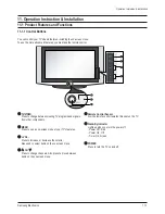
Page 110: ...hange between viewing TV programs and signals from other components MENU Press to see an on screen menu of your TV s features VOL Press to increase or decrease the volume Also used to select items on...

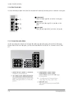
Page 111: ...jacks you can connect three different A V components i e a VCR and a DVD 2 VCRs etc 11 1 2 Side Panel Jacks You can use the side panel jacks to connect an A V component that is used only occasionally...

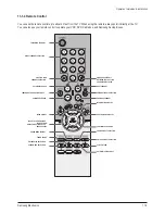
Page 112: ...CHANNEL SELECTION VOLUME INCREASE TEMPORARY SOUND SWITCH OFF MENU DISPLAY MOVE TO THE REQUIRED MENU OPTION ADJUST AN OPTION VALUE RESPECTIVELY TURBO SOUND EXTERNAL INPUT SELECTION AUTOMATIC SWITCH OF...

Page 113: ...EL TELETEXT DISPLAY MIX BOTH TELETEXT INFORMATION AND THE NORMAL BROADCAST PIP ON OFF FASTEXT TOPIC SELECTION TELETEXT SUB PAGE TELETEXT MODE SELECTION LIST FLOF TELETEXT SIZE SELECTION SUB PICTURE PI...

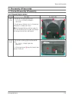
Page 114: ...6 Tap the upper part of the Back Cover 2 or 3 times and pull the Back Cover to separate it from the unit Notice Disassemble the product after disconnecting the power cord and discharge the unit to pre...

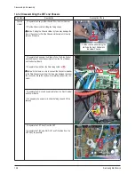
Page 115: ...Cabinet and the System Board Separate the wire from the Wire fixing holder at Notice Since there is a clip to connect the Connector Header in the Wire Connector pulling it by force may damage the clip...

Page 116: ...t to the hole and pull the wire Notice Take care when separating the wires because pulling the wires by force may damage the socket In addition separate the wires on a flat and clean surface so as to...

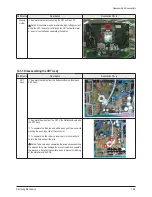
Page 117: ...Board Separate the cable from the Splitter and the Tuner First separate the cable from the Splitter using a tool such as nippers Notice Since pulling the wire by force may damage the coating of the w...

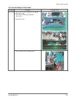
Page 118: ...scription Description Photo Power Board Remove the 4 screws to separate the holder fixing the Deflection Board Holder RH B M4 L15 ZPC BLK SWRCH18A 6003 001026 Separate the holder Separate the cable fr...

Page 119: ...12 6 Samsung Electronics MEMO...

Page 120: ...lowering of top and bottom LA7845 N S TRANS etc 3 HRS Horizontal Raster Shift Correction Circuit A correction circuit of Linearity distortion on the left and right side of a picture which is caused b...

Page 121: ...Circuit Description 13 2 Samsung Electronics Vertical Bias N S Correction Circuit D F Correction Circuit Horizontal HRS Circuit E W Correction Circuit...

Page 122: ...g vertically in a shape of a spool because of the strong bias at four corners which are the farthest from the center Correction effect to the amount of a correction signal can be made by crossing Para...

Page 123: ...V m 0 1 2 H C 1 1 C D V m 0 6 1 2 2 V r e t l i F N O g n i h t o o m S L L U F W B t e s f f O V 0 0 1 H C V 0 0 0 0 0 2 H C V 0 0 3 H C V 0 0 4 H C h t g n e L d r o c e R K 0 0 1 n i a M K 0 1 m o...

Page 124: ...consists of R407 D415 D407 SW401 C415 L404 If switch SW401 Service S W to the direction of R407 it raises the C426 CS condenser voltage through D415 and the picture moves to right If switch SW401 to...

Page 125: ...t using a comparator The advantage of this PWM Control method is that POWER Loss hardly occurs and generates little heat when using low H S Input E W signal to terminal no 3 5 of IC401 KA393 and carri...

Page 126: ...COMP likewise controls the vertical correction vector and operates in the same mechanism as H COMP PIN COMP is a function which corrects the movement of four corners of a picture If the capacity value...

Page 127: ...27W201 Regulator 78RM33D 3 3V Regulator Regulator 18 DPAK 1 8V Regulator Regulator 4931 TO 252 5V Regulator Main Board Items Descriptions Remarks BRIDGE DIODE GSIB660 Didode SLA1004L Trans Switching 5...

Page 128: ...ching video from a DVD VCR computer or game console through a wide TV by selecting the aspect ratio to normal 4 3 or wide 21 9 the left and right or top and bottom of the picture will not be displayed...

Page 129: ...nal Input External Input is connecting video devices such as a VCR camcorder DTV receiver DVD etc as a video source Satellite Broadcast Satellite Broadcast transmits programs via satellite so that the...

Reviews: