


RT8239A/B/C
22
DS8239A/B/C-06 October 2012
www.richtek.com
©
Copyright 2012 Richtek Technology Corporation. All rights reserved. is a registered trademark of Richtek Technology Corporation.
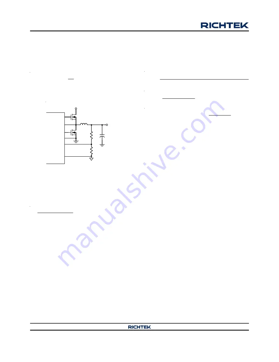
Output Voltage Setting (FBx)
Connect a resistive voltage divider at the FBx pin between
V
OUTx
and GND to adjust the output voltage between 2V
and 5.5V (Figure 7). Choose R2 to be approximately 10k
Ω
,
and solve for R1 using the equation :
⎛
⎞
⎛
⎞
=
× +
⎜
⎟
⎜
⎟
⎝
⎠
⎝
⎠
OUT
FBx
R1
V
V
1
R2
where V
FBx
is 2V (typ.).
UGATEx
PHASEx
LGATEx
PGND
FBx
GND
R1
R2
VOUTx
V
IN
Figure 7. Setting V
OUTx
with a resistive voltage divider
Output Inductor Selection
The switching frequency (on-time) and operating point (%
ripple or LIR) determine the inductor value as shown
below :
×
−
=
×
ON
IN
OUTx
LOAD(MAX)
t
(V
V
)
L
LIR I
where LIR is the ratio of the peak-to-peak ripple current to
the average inductor current.
Find a low-loss inductor having the lowest possible DC
resistance that fits in the allotted dimensions. Ferrite cores
are often the best choice, although powdered iron is
inexpensive and can work well at 200kHz. The core must
be large enough not to saturate at the peak inductor
current, I
PEAK
:
I
PEAK
= I
LOAD(MAX)
+ [ (LIR / 2) x I
LOAD(MAX)
]
The calculation above shall serve as a general reference.
To further improve transient response, the output
inductance can be further reduced. Of course, besides
the inductor, the output capacitor should also be
considered when improving transient response.
Output Capacitor Selection
The capacitor value and ESR determine the amount of
output voltage ripple and load transient response. Thus,
the capacitor value must be greater than the largest value
calculated from below equations.
Δ
× ×
+
=
⎡
⎤
×
×
×
−
⎣
⎦
2
LOAD
ON
OFF(MIN)
SAG
OUT
IN
ON
OUTx ON
OFF(MIN)
( I
)
L (t
t
)
V
2 C
V
t
V
(t
+ t
)
(
)
2
LOAD
SOAR
OUT
OUTx
I
L
V
2 C
V
Δ
×
=
×
×
−
⎛
⎞
=
×
×⎜
⎟
×
×
⎝
⎠
P P
LOAD(MAX)
OUT
1
V
LIR I
ESR +
8 C
f
where V
SAG
and V
SOAR
are the allowable amount of
undershoot and overshoot voltage during load transient,
V
p-p
is the output ripple voltage, and t
OFF(MIN)
is the
minimum off-time.
Thermal Considerations
For continuous operation, do not exceed absolute
maximum junction temperature. The maximum power
dissipation depends on the thermal resistance of the IC
package, PCB layout, rate of surrounding airflow, and
difference between junction and ambient temperature. The
maximum power dissipation can be calculated by the
following formula :
P
D(MAX)
= (T
J(MAX)
−
T
A
) /
θ
JA
where T
J(MAX)
is the maximum junction temperature, T
A
is
the ambient temperature, and
θ
JA
is the junction to ambient
thermal resistance.
For recommended operating condition specifications, the
maximum junction temperature is 125
°
C. The junction to
ambient thermal resistance,
θ
JA
, is layout dependent. For
WQFN-20L 3x3 packages, the thermal resistance,
θ
JA
, is
30
°
C/W on a standard JEDEC 51-7 four-layer thermal test
board. The maximum power dissipation at T
A
= 25
°
C can
be calculated by the following formula :
P
D(MAX)
= (125
°
C
−
25
°
C) / (30
°
C/W) = 3.33W for
WQFN-20L 3x3 package
The maximum power dissipation depends on the operating
ambient temperature for fixed T
J(MAX)
and thermal


