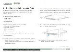
RZ/A2M SUB Board RTK79210XXB00000BE
3. Operating specifications
R20UT4398EJ0100 Rev.1.00
3-25
2018.10.11
Table 3.2.2
Mounted RTK79210XXB00000BE Switch Overview
Numbers
Function
Note
SW1
Power supply switch
SW2
NMI switch
Refer to section 2.6 for details.
SW3
IRQ0 switch
SW4
Key input switch
Refer to section 2.14 for details.
SW5
Key input switch
SW6
DIP switch for system settings
Refer to Table
for further details
Table 3.2.3
Explanation of DIP Switch Functions (SW6)
Numbers
Settings
Function
SW6-1
P9_[7
:0]
、
P8_[7
:1]
、
P2_2
、
P2_0
、
P1_3
、
P1_[1
:0]
、
P0_[6
:0]
、
P6_7
、
P6_5
、
P7_[1
:0]
、
P7[5
:3] connection address
selection
OFF
SDRAM#/Other =
“
H
”
Used as DRP, audio, UART, and USB interface pins
ON
SDRAM#/Other =
“
L
”
Used as SDRAM control pin
SW6-2
P8_4
、
P8_[7:6]
、
P6_4
、
P9_[6:3] connection
address selection
OFF
DRP#/Audio =
“
H
”
Used as audio interface pin
ON
DRP#/Audio =
“
L
”
Used as DRP pin
SW6-3
P9_[1
:0]
、
P1_0
、
P7_5
connection address selection
OFF
DRP#/Other =
“
H
”
Used as UART and USB interface pins
ON
DRP#/Other =
“
L
”
Used as DRP pin
SW6-4
P6_[3:1]
、
PE_[6:0]
connection address selection
OFF
Ether1#/CEU =
“
H
”
Used as CEU pin
ON
Ether1#/CEU =
“
L
”
Used as Ethernet PHY1 control pin
SW6-5
P3_[5:1]
、
PH_5
、
PK_[4:0]
connection address selection
OFF
Ether2#/NAND =
“
H
”
Used as FLCTL pin
ON
Ether2#/NAND =
“
L
”
Used as Ethernet PHY2 control pin
SW6-6
PJ_[7:6] connection
address selection
OFF
VDC6#/NAND =
“
H
”
Used as FLCTL pin
ON
VDC6#/NAND =
“
L
”
Used as VDC6 pin
SW6-7
P7_[7:4] connection
address selection
OFF
VDC6#/Other =
“
H
”
NC
ON
VDC6#/Other =
“
L
”
Used as VDC6 pin
SW6-8
OFF
NC
ON
NC
SW6-9
P5_3
OFF
P5_3 =
“
H
”
Generic input port P5_3 =
“H”
ON
P5_3 =
“
L
”
Generic input board P5_3 =
“
L
”
SW6-10
PC_2
OFF
PC_2 =
“
H
”
Generic input port PC_2 =
“H”
ON
PC_2 =
“
L
”
Generic input port PC_2 =
“L”
[Note] indicates default setting.
Be sure to turn the board power to off before altering the DIP switch setting.