background image

Isolated optocoupler outputs

The Isolated optocoupler output stage of the DM6854HR consists of 3 major parts: 

1. Output data register
2. Schmidt triggers
 
3. Optocouplers.

1. Output data register

The four bit output register holds the output pattern for the output stage. Data can

be updated and read from address (BA+3), bits 4-8. The lower bits (1-4) hold the configuration
bits of your DM6854HR. Make sure these bits are unchanged when writing to this register. 
To avoid accidental changes in configuration read first data in the register (BA+3) before writing
to it. 

2. Schmidt triggers

The output of the optocoupler has a Schmidt trigger to condition the output of the

optocouplers, this will reduce false triggering. 

3. Optocouplers

Small SMD-optocouplers are used to isolate each channel of the isolated outputs.

Individual optocouplers are used for each channel. The optocouplers are directly connected 
to the Output data register. The optocouplers are connected in a non inverting configuration
in open collector configuration. The maximum switching current is 8mA at 30V.

DM5854HR/DM6854HR                                  Page 26                (c) RTD Finland Oy 1996-2001

Summary of Contents for DM5854HR

Page 1: ...e User s Manual Real Time Devices Finland Oy Real Time Devices Finland Oy Lepolantie 14 FIN 00660 Helsinki Finland Tel 358 9 346 4538 Fax 358 9 346 4539 Email sales rtdfinland fi URL www rtdfinland fi DM5854HR DM6854HR c RTD Finland Oy 1996 2001 ...
Page 2: ...se of this manual or from the related software RTD Finland Oy also reserves the right to alter the contents of this manual as well as features and specifications of this product at any time without prior notice Published by Real Time Devices Finland Oy Lepolantie 14 FIN 00660 Helsinki Finland Copyright 1996 2001 by RTD Finland Oy All rights reserved Printed in Finland DM5854HR DM6854HR c RTD Finla...

Page 3: ...ETTINGS Factory configured jumper settings Base Address jumpers Interrupts and interrupt channels Pull up or Pulldown jumpers Isolated input range selection jumpers CHAPTER 2 BOARD INSTALLATION Board installation External I O connections Isolated Input Output Connector 50 pin RTD Expansion Connector CHAPTER 3 HARDWARE DESCRIPTION Digital I O 8255 Programmable digital I O Isolated optocoupler input...

Page 4: ...setting bits in a port Initializing the 8255 PPI Isolated Digital Input programming Isolated Digital Output programming Trigger Output programming Interrupts What is an interrupt Interrupt request lines 8259 Programmable interrupt controller Interrupt mask register IMR End Of Interrupt EOI Command What exactly happens when an interrupt occurs Using interrupts in your program Writing an interrupt s...

Page 5: ...List of Illustrations DM5854HR DM6854HR Page 3 c RTD Finland Oy 1996 2001 ...

Page 6: ...atible general purpose digital I O lines which can be directly interfaced with external devices or signals to interface to alphanumerical displays sense switch closures trigger digital events or activate solid state relays These lines may be pulled down or pulled up or pulled down with 10K Ohm resistor networks Installation procedures will be described later in this manual Isolated digital inputs ...

Page 7: ...rminal block Please consult the factory for more details on different connector options What comes with your board You receive the following items in your DM6854HR package DM5854HR or DM6854HR Isolated digital interface module User s manual Note Latest software and drivers can be downloaded from our website If any item is missing or damaged please call Real Time Devices Finland Customer service de...

Page 8: ...ures even in the most demanding applications When you need help This manual and all the example programs will provide you with enough information to fully utilize all the features on this board If you have any problems installing or using this board contact our Technical Support Department 358 9 346 4538 during European business hours or send a FAX to 358 9 346 4539 or Email to sales rtdfinland fi...

Page 9: ...ngs you can change to suit your application and I O configuration setup The board is factory configured with a 24V input range configuration The factory settings are listed and shown in the diagram in the beginning of this chapter DM5854HR DM6854HR Page 7 c RTD Finland Oy 1996 2001 ...

Page 10: ...uit your specific application Table 1 1 Factory jumper settings see figure 1 1 for detailed locations JUMPER DESCRIPTION NUMBER OF FACTORY SETTING NAME OF JUMPER JUMPERS JUMPERS INSTALLED BASE BASE ADDRESS 5 300h INSTALLED IRQ INTERRUPT CHANNEL 6 5 PU PD PU PD FOR PPI PORTS 3 Terminal PULLDOWN IN1 8 INPUT RANGE FOR 3 24V RANGE ISOLATED INPUTS 1 8 Figure 1 1 Board layout showing jumper locations DM...

Page 11: ...you set up the base address first using the jumpers marked BASE which let you choose from 32 different I O addresses in your computers I O map Should the factory installed setting of 300H be unusable for your system configuration you may change this setting to another using the options illustrated in Table 1 2 The table shows the switch settings and their corresponding values in hexadecimal values...

Page 12: ...0 832 1 0 1 0 0 250 592 0 0 1 0 1 350 848 1 0 1 0 1 260 608 0 0 1 1 0 360 864 1 0 1 1 0 270 624 0 0 1 1 1 370 880 1 0 1 1 1 280 640 0 1 0 0 0 380 896 1 1 0 0 0 290 656 0 1 0 0 1 390 912 1 1 0 0 1 2A0 672 0 1 0 1 0 3A0 928 1 1 0 1 0 2B0 688 0 1 0 1 1 3B0 944 1 1 0 1 1 2C0 704 0 1 1 0 0 3C0 960 1 1 1 0 0 2D0 720 0 1 1 0 1 3D0 976 1 1 1 0 1 2E0 736 0 1 1 1 0 3E0 992 1 1 1 1 0 2F0 752 0 1 1 1 1 3F0 10...

Page 13: ...errupt to one of the 6 interrupt channels available on the XT AT bus Fig 1 3 Interrupt selection jumpers The interrupt is caused by an external trigger event that has transferred the storage latch data to the output latch of the isolated digital output stage DM5854HR DM6854HR Page 11 c RTD Finland Oy 1996 2001 ...

Page 14: ...e active before the 8255 is initialized Figure 1 4 shows both Ports A B and C set in the Pull down configuration Fig 1 4 Pull up and Pull down jumpers for Ports A B and C Inputs pulled down when jumpers in right hand position see above PC4 PC7 Optocoupler isolated inputs Factory setting 24V range The Optocoupler inputs can be jumper configured for different input ranges Each channel can be set for...

Page 15: ...Fig 1 5 Optocoupler input range jumpers set for 24V input range Fig 1 6 Optocoupler input stage layout of the DM6854HR DM5854HR DM6854HR Page 13 c RTD Finland Oy 1996 2001 ...

Page 16: ...system Direct interface to PC 104 systems as well as EUROCARD boards is provided This chapter tells you step by step how to install your board into your system After completing the installation use the diagnostic software to fully verify that your board is working DM5854HR DM6854HR Page 14 c RTD Finland Oy 1996 2001 ...

Page 17: ... operation and erratic response General installation guidelines 1 Turn OFF the power to your computer 2 Touch the grounded metal housing of your computer to discharge any antistatic buildup and then remove the board from its antistatic bag 3 Hold the board by it s edges and install it in an enclosure or place it on the table on an antistatic surface 4 Connect the board to the data acquisition boar...

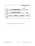
Page 18: ...Fig 2 1 DM5854HR integrated with a PC 104 dataModule stack DM5854HR DM6854HR Page 16 c RTD Finland Oy 1996 2001 ...

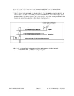
Page 19: ...or adapter Assemble your PC 104 dataModules on a RTD single board EUROCARD computer and install the system in a 19 enclosure Multiple DM5854HR boards can easily be connected to this system See figure 2 2 Fig 2 2 19 Eurocard rack installation with an integrated PC 104 dataModule and EUROCARD cpuModule computer system DM5854HR DM6854HR Page 17 c RTD Finland Oy 1996 2001 ...

Page 20: ... pinout and figure 2 3b shows the pinout of the same connector using a header connector Pin 1 is to the left side of the connector ALL SIGNALS ARE ISOLATED 1 IN1 2 IN1 3 IN2 4 IN2 5 IN3 6 IN3 7 IN4 8 IN4 9 IN5 10 IN5 11 IN6 12 IN6 13 IN7 14 IN7 15 IN8 16 IN8 17 OUT1_COLLECTOR 18 OUT1_EMITTER 19 OUT2_COLLECTOR 20 OUT2_EMITTER 21 OUT3_COLLECTOR 22 OUT3_EMITTER 23 OUT4_COLLECTOR 24 OUT4_EMITTER Fig 2...

Page 21: ...IN7 27 28 IN7 29 30 IN8 31 32 IN8 33 34 OUT1_COLLECTOR 35 36 OUT1_EMITTER 37 38 OUT2_COLLECTOR 39 40 OUT2_EMITTER 41 42 OUT3_COLLECTOR 43 44 OUT3_EMITTER 45 46 OUT4_COLLECTOR 47 48 OUT4_EMITTER Fig 2 3b Isolated Input Output interface using a 48 pin header connector DM5854HR DM6854HR Page 19 c RTD Finland Oy 1996 2001 ...

Page 22: ...PC2 5 6 DGND PC3 7 8 DGND PC4 9 10 DGND PC5 11 12 DGND PC6 13 14 DGND PC7 15 16 DGND PB0 17 18 DGND PB1 19 20 DGND PB2 21 22 DGND PB3 23 24 DGND PB4 25 26 DGND PB5 27 28 DGND PB6 29 30 DGND PB7 31 32 DGND PA0 33 34 DGND PA1 35 36 DGND PA2 37 38 DGND PA3 39 40 DGND PA4 41 42 DGND PA5 43 44 DGND PA6 45 46 DGND PA7 47 48 DGND 5V fused 49 50 DGND Fig 2 4 50 pin expansion interface connector pinout DM5...

Page 23: ...r 3 Hardware Description describes the major features of the DM6854HR the 8255 based digital I O isolated optocoupler inputs isolated optocoupler outputs interrupts and output triggering DM5854HR DM6854HR Page 21 c RTD Finland Oy 1996 2001 ...

Page 24: ... This chapter describes the major features of the DM6854HR the 8255 based digital I O isolated optocoupler inputs isolated optocoupler outputs interrupts and output triggering Fig 3 1 DM6854HR Block diagram DM5854HR DM6854HR Page 22 c RTD Finland Oy 1996 2001 ...

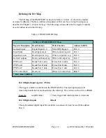
Page 25: ...e operating modes Mode 0 Basic I O Lets you use simple input output functions for a port Data is written to or read from the specified port Mode 1 Strobed Input Output Lets you transfer data I O from port A in conjunction with strobed or handshake signals Mode 2 Strobed bi directional input output Lets you communicate with an external device through port A Handshaking is similar to mode 1 Availabl...

Page 26: ...DM5854HR DM6854HR Page 24 c RTD Finland Oy 1996 2001 ...

Page 27: ...ge on the isolated digital input will be interpreted as a logical 1 To avoid false triggering on the inputs special Schmidt trigger buffers are used to provide reliable and precise switching of the inputs 3 Input bit mask stage The programmable input processing section of the DM6854HR includes an input bit mask filter stage This mask may be is used to select bits or groups of interesting bits for ...

Page 28: ...avoid accidental changes in configuration read first data in the register BA 3 before writing to it 2 Schmidt triggers The output of the optocoupler has a Schmidt trigger to condition the output of the optocouplers this will reduce false triggering 3 Optocouplers Small SMD optocouplers are used to isolate each channel of the isolated outputs Individual optocouplers are used for each channel The op...

Page 29: ...n the 50 pin expansion connector Pin 2 You may use this to trigger other devices or other boards in your system such as the isolated digital output board and DM6854HR The polarity of this trigger signal is programmable and is driven by a tristate buffer This enables several boards to drive the same trigger output signal Interrupts The DM6854HR has an interrupt available to indicate an external tri...

Page 30: ...ter shows you how to program and use your DM6854HR It provides a complete detailed description of the I O map and a detailed discussion of programming operations to aid you in application programming DM5854HR DM6854HR Page 28 c RTD Finland Oy 1996 2001 ...

Page 31: ...t inv reg Write to input inv reg BA 2 Isolated outputs Read conf output reg Write conf output reg BA 3 PPI Port A Reads Port A data Writes Port A data BA 4 PPI Port B Reads Port B data Writes Port B data BA 5 PPI Port C Reads Port C data Writes Port C data BA 6 PPI Control Byte Reserved Writes to Control byte BA 7 BA Base Address BA 0 Digital input register Write The trigger condition is latched o...

Page 32: ...it changes state from condition 0x3E Step 1 Mask required bits outp BA 1 0x7F 0 1 1 1 1 1 1 1 Step 2 Set inversion register outp BA 2 0x3E 0 0 1 0 1 1 1 0 BA 2 Input inversion register Read Performing a read to the input inversion register address will return the current data stored in the register BA 3 Configuration digital output register Write 0 after reset BIT 0 1 External host IRQ enabled 0 E...

Page 33: ...hrough J5 to the external devices BA 6 PPI Port C Read Write Transfers the 4 bit low nibble of the Port C digital input and output data between the module and an external device A read transfers data from the external device through connector J5 and into bits 0 7 of port C a write transfers the written data bits 0 7 from port C through J5 to the external devices BA 7 PPI Control Byte Write only Wh...

Page 34: ... 1 C lower Input When bit 7 is set to 0 a write can program individual lines of port C D7 0 Active Set Reset Function bit D3 D2 D1 Bit Select 0 0 0 PC0 0 0 1 PC1 0 1 0 PC2 0 1 1 PC3 1 0 0 PC4 1 0 1 PC5 1 1 0 PC6 1 1 1 PC7 D0 1 Set bit to 1 0 Set bit to 0 DM5854HR DM6854HR Page 32 c RTD Finland Oy 1996 2001 ...

Page 35: ...et bits in an I O port you must be careful not to alter the status of other bits You can preserve the status of all the bits you do not wish to change by proper use of the bitwise AND and OR operators Using and or operators single or multiple bits can easily be set or cleared in one line operations 1 To clear a single bit in a port AND the current value of the port with the value B where B 255 2 e...

Page 36: ...ss BA 0 The DM6854HR features more advanced modes of input pattern or bit change recognition to reduce software overhead This is possible with the hardware interrupt generated by the onboard comparison logic The following two subsections will illustrate how to program the different modes of the isolated digital input port 1 Software controlled direct read in_data inp BA Loads data from inputs into...

Page 37: ...n and output data and write to port outp BA 3 out_data conf_data write to correct address This code can be compressed into more elegant and optimum code The steps above illustrate the logic of operation Trigger output programming As described in the previous sections an external trigger may be used to indicate to the host or other devices that a predetermined input condition has occurred Before yo...

Page 38: ...rising edge transition on one of these lines will be latched into the interrupt controller The interrupt controller checks to see if the interrupts are to be acknowledged from that IRQ and if another interrupt is being processed it decides if the new request should supersede the one in progress or if it has to wait until the one in progress is done The priority level of the interrupt is determined...

Page 39: ...cult as it may seem especially when programming under DOS The following discussion will cover programming under DOS Note that even the smallest mistake in your interrupt program may cause the computer to hang up and will only restart after a reboot This can be frustrating and time consuming Writing an Interrupt Service Routine ISR The first step in adding interrupts to your software is to write an...

Page 40: ...at use the screen read keyboard input and any file I O routines should not be used in ISR s The same problem of reentrancy exists for many floating point emulators as well meaning you should avoid floating point mathematical operations in your ISR Note that the problem of reentrancy exists no matter what programming language you use Even if you are writing your ISR in Assembly language DOS and man...

Page 41: ...us if your DM6854HR is using IRQ5 it corresponds to vector number 13 Before you install your ISR temporarily mask out the IRQ you will be using This prevents the IRQ from requesting an interrupt while you are installing and initializing your ISR To mask the IRQ read the current IMR at I O port 21h and set the bit that corresponds to tout IRQ The IMR is arranged so that bit 0 is for IRQ0 and bit 7 ...

Page 42: ...me for IRQ void interrupt far old_IRQ1_dispatcher es ds di si bp sp bx dx cx ax ip cs flags Variable to store old IRQ_Vector void far _interrupt new_IRQ1_handler void Function init_irq_handlers Inputs Nothing Returns Nothing Purpose Set the pointers in the interrupt table to point to our funtions ie setup for ISR s void init_irq_handlers void _disable old_IRQ1_handler _dos_getvect IRQ1_VECTOR 8 _d...

Page 43: ...m Inputs Nothing Returns Nothing Purpose Restore interrupt vector table void restore void Restore the old vectors _disable _dos_setvect IRQ1_VECTOR 8 old_IRQ1_handler outp 0x21 Gi_old_mask _enable DM5854HR DM6854HR Page 41 c RTD Finland Oy 1996 2001 ...

Page 44: ...ranges jumper selectable 4 Triggering Voltages 5V range 3 3V approx 12V range 8 5V approx 24V range 20V approx Isolation Voltage 1 500V Rms Optocoupler switching current 10mA Typical 16mA Maximum Digital outputs isolated Number of lines 4 Isolation Voltage 1 500V Rms Output stage Open collector 8mA 30V Connectors Isolated I O 24 terminal screw terminal connector Optional header connector 48 Pin No...

Page 45: ...NOTES C RTD Finland Oy 1996 2001 DOC DM6854 SAM DM5854HR DM6854HR Page 43 c RTD Finland Oy 1996 2001 ...

Reviews: