Hardware Connections
Step 1 — Prepare the Prototyping Board
To facilitate handling the Prototyping Board, snap in the
four standoffs to the four holes at the corners from the
bottom side of the Prototyping Board as shown in
Figure 1.
NOTE:
The hole at the bottom left of the Prototyping
Board is used to mount the RCM4300, so use the
hole immediately above it for the standoff.
Step 2 — Insert the miniSD™ Card
Insert the
miniSD™ Card
.into the
miniSD
Card holder on
the RCM4300. The card is designed to fit easily only one way — do
not
bend
the card or force it into the slot.You will sense a soft click once the card is
inserted completely.
Step 3 — Attach RCM4300 Module to Prototyping Board
Step 4 — Connect Programming Cable
The programming cable connects the RCM4300 to the PC running Dynamic C to download programs and to mon-
itor the RCM4300 module during debugging.
Connect the 10-pin connector of the programming cable labeled
PROG
to header J1 on the RCM4300 as shown in
Figure 3. Be sure to orient the marked (usually red) edge of the cable towards pin 1 of the connector. (Do not use
the
DIAG
connector,
which is presently not supported by the RCM4300
.)
Turn the RCM4300 module so that the
mounting holes line up with the correspond-
ing holes on the Prototyping Board. Insert
the metal standoffs as shown in Figure 2,
secure them from the bottom using the three
screws and washers, then insert the module’s
header J4 on the bottom side into socket
RCM1 on the Prototyping Board.
NOTE:
It is important that you line up the
pins on header J4 of the module
exactly with socket RCM1 on the Pro-
totyping Board. The header pins may
become bent or damaged if the pin
alignment is offset, and the module
will not work. Permanent electrical
damage to the module may also result
if a misaligned module is powered up.
Press the module’s pins firmly into the Proto-
typing Board socket—press down in the area
above the header pins. For additional integ-
rity, you may secure the RCM4300 to the
standoffs from the top using the remaining
three screws and washers.
Figure 2. Install the RCM4300 Module
on the Prototyping Board
Figure 1. Insert Standoffs
D1
R1
PWR
DS1
GND
J1
U1
C1
GND
C2
JP
1
C3
D2
JP
2
C4
+3
.3
V
J2
R2
BT1
1
S1
RESET
RX
D T
XD
TX
C
RX
C
GN
D
J4
UX
29
RX81
RX
87
CX
41
RX83
RX11
CX
39
UX30
UX10
UX12
UX14
UX16
RX79
CX
29
CX
17
RX67
UX
45
RX
85
GND
GND
GND
1
R24
R22
R21
R23
CX23 RX77
1 R27 R28
JP25
CX25
RX75
RX73
CX27
DS3
S3
S2
DS2
J3
UX49
UX4
UX47
+5 V
GND
+3.3 V
RCM1
U2
/RST_OUT
/IOWR
VBAT
EXT
PA1
PA3
PA5
PA7
PB1
PB3
PB5
PB7
PC1
PC3
PC5
PC7
PE1
PE3
PE5
PE7
PD1
LN1
PD3
LN3
PD5
LN5
PD7
LN7
VREF
GND
/I
ORD
/
RST_IN
PA0
PA2
PA4
PA6
PB0
PB2
PB4
PB6
PC0
PC2
PC4
PC6
PE0
PE2
PE4
PE6
PD0
LN0
PD2
LN2
PD4
LN4
PD6
LN6
CVT
AGND
JP
24
JP
23 C1
4
C1
2
C1
0 C8 C7 C9 C11 C13
R10
R8 R6 R4 R3 R5 R7
R20
R1
8
R1
6
R1
4
R1
3
R1
5
R1
7
R29
JP
11
JP
15
JP
19
JP
21
JP2
2
JP2
0
JP1
7
JP
13
R19
R9
RX57
RX55
RX97
RX49
UX
33
UX
31
RX
89
UX3
UX
37
UX
42
UX
41
RX
63
RX
65
RX
61
RX59
R2
6
R25
Q1
C15
C1
9
C2
0
U3
C18
C1
7
JP16
JP6
JP5
JP12
JP4
JP3
JP14
JP8
JP7
JP18
JP9
JP10
C16
L1C6
C5
AG
ND
CV
T
LN
6IN
LN
4IN
LN
2IN
LN
0IN
VR
EF
LN
7IN
LN
5IN
LN
3IN
LN
1IN
AG
ND
AG
ND
R1
1
R1
2
RX
47
RX43
D1
R1
PWR
DS1
GND
J1
U1
C1
GND
C2
JP1
C3
D2
JP2
C4
+3.3 V
J2
R2
BT1
1
S1
RESET
RXD
TXD
TXC RXC
GND
J4
UX29
RX81
RX87
CX41
RX83
RX11
CX39
UX30
UX10
UX12
UX14
UX16
RX79
CX29
CX17
RX67
UX45
RX85
GND
GND
GND
1
R24
R22
R21
R23
CX23 RX77
1
R27 R28
JP25
CX25
RX75
RX73
CX27
DS3
S3
S2
DS2
J3
UX49
UX4
UX47
+5 V
GND
+3.3 V
RCM1
U2
/RST_OUT
/IOWR
VBAT
EXT
PA1
PA3
PA5
PA7
PB1
PB3
PB5
PB7
PC1
PC3
PC5
PC7
PE1
PE3
PE5
PE7
PD1
LN1
PD3
LN3
PD5
LN5
PD7
LN7
VREF
GND
/I
ORD
/
RST_IN
PA0
PA2
PA4
PA6
PB0
PB2
PB4
PB6
PC0
PC2
PC4
PC6
PE0
PE2
PE4
PE6
PD0
LN0
PD2
LN2
PD4
LN4
PD6
LN6
CVT
AGND
JP24
JP23
C14
C12
C10
C8
C7
C9
C1
1
C13
R10
R8
R6
R4
R3
R5
R7
R20
R18
R16
R14
R13
R15
R17
R29
JP1
1
JP15
JP19
JP21
JP22 JP20
JP17
JP13
R19
R9
RX57
RX55
RX97
RX49
UX33
UX31
RX89
UX3
UX37
UX42
UX41
RX63
RX65
RX61
RX59
R26
R25
Q1
C15
C19
C20 U3
C18
C17
JP16
JP6
JP5
JP12
JP4
JP3
JP14
JP8
JP7
JP18
JP9
JP10
C16
L1C6
C5
AGND
CVT
LN6IN
LN4IN
LN2IN
LN0IN
VREF
LN7IN
LN5IN
LN3IN
LN1IN
AGND
AGND
R1
1
R12
RX47
RX43
J1
R1
R2
R19
R3
R4
C3
L1
C1
C2
Y1
4
1
3
R16
R17
C4
C8
C5
C6
C7
R20
U2
R21
R22
R23
C13
C12
L2
C10
JP15
C21
U7
R38
J2
R37
R36
C22
DS1
LINK
SPEED
FDX
DS3
DS2
R39
R40
R41
R35
C23
R34
U6
R33
R31
R32
D1
R66
C14
C11
C9
R7
R6
DS4
R42
J3
U18
R65
R67
R64
R29
R68
R69
R30
R24
C15 C16 R28 R27 R26
R25
C20
U5
JP12
JP13
JP14
R71
R70
R5
JP1
JP2
R72 JP3
JP4
JP5
JP6
JP7
JP8
JP9
JP10
JP11
U3 R8
R9
Q2
Q3
C91
C93
U1
R10
R1
1
R13
R12
R14
R15
C17
C18
C19
C92
C90
RCM4300
RCM1
Line up mounting
holes with holes
on Prototyping Board.
Insert standoffs
between
mounting holes and
Prototyping Board.
Programming
Header
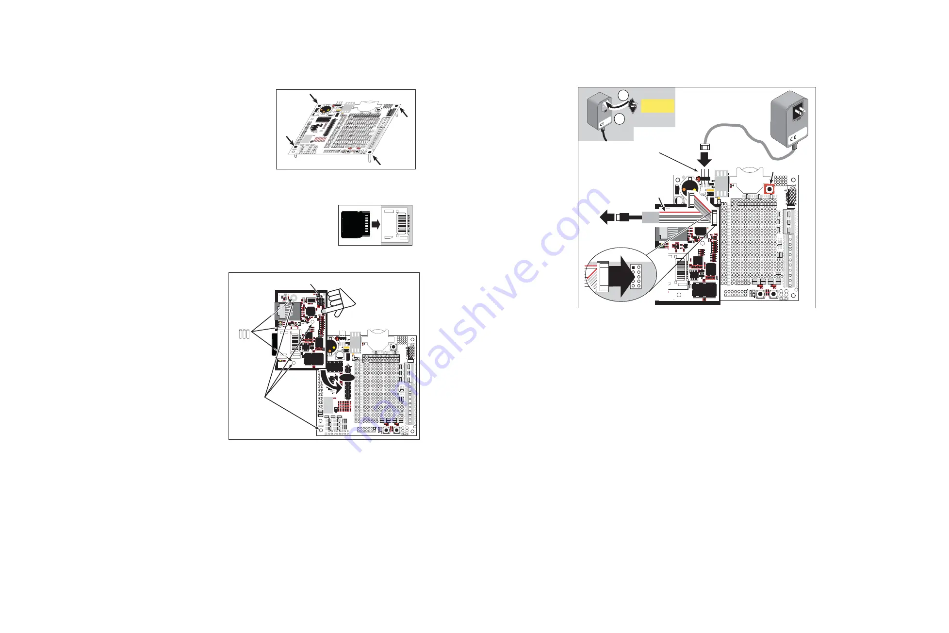
Figure 3. Connect Programming Cable and Power Supply
Connect the other end of the programming cable to an available USB port on your PC or workstation.
Your PC should recognize the new USB hardware, and the LEDs in the shrink-wrapped area of the USB
programming cable will flash — if you get an error message, you will have to install USB drivers. Drivers
for Windows XP are available in the Dynamic C
Drivers\Rabbit USB Programming Cable\
WinXP_2K
folder — double-click
DPInst.exe
to install the USB drivers. Drivers for other operating
systems are available online at
www.ftdichip.com/Drivers/VCP.htm
.
Step 5 — Connect Power
Once all the other connections have been made, you can connect power to the Prototyping Board.
First, prepare the AC adapter for the country where it will be used by selecting the plug. The RCM4300
Development Kit presently includes Canada/Japan/U.S., Australia/N.Z., U.K., and European style plugs.
Snap in the top of the plug assembly into the slot at the top of the AC adapter as shown in Figure 3, then
press down on the spring-loaded clip below the plug assembly to allow the plug assembly to click into
place. Release the clip to secure the plug assembly in the AC adapter.
Connect the AC adapter to 3-pin header J1 on the Prototyping Board as shown in Figure 3. The connector
may be attached either way as long as it is not offset to one side—the center pin of J1 is always connected
to the positive terminal, and either edge pin is ground.
Plug in the AC adapter. The
PWR
LED on the Prototyping Board next to the power connector at J1 should
light up. The RCM4300 and the Prototyping Board are now ready to be used.
NOTE:
A
RESET
button is provided on the Prototyping Board next to the battery holder to allow
a hardware reset without disconnecting power.
D1
R1
PWR
DS1
GND
J1
U1
C1
GND
C2
JP1
C3
D2
JP2
C4
+3.3 V
J2
R2
BT1
1
S1
RESET
RXD
TXD
TXC RXC
GND
J4
UX29
RX81
RX87
CX41
RX83
RX11
CX39
UX30
UX10
UX12
UX14
UX16
RX79
CX29
CX17
RX67
UX45
RX85
GND
GND
GND
1
R24
R22
R21
R23
CX23 RX77
1
R27 R28
JP25
CX25
RX75
RX73
CX27
DS3
S3
S2
DS2
J3
UX49
UX4
UX47
+5 V
GND
+3.3 V
RCM1
U2
/RST_OUT
/IOWR
VBAT
EXT
PA1
PA3
PA5
PA7
PB1
PB3
PB5
PB7
PC1
PC3
PC5
PC7
PE1
PE3
PE5
PE7
PD1
LN1
PD3
LN3
PD5
LN5
PD7
LN7
VREF
GND
/I
ORD
/
RST_IN
PA0
PA2
PA4
PA6
PB0
PB2
PB4
PB6
PC0
PC2
PC4
PC6
PE0
PE2
PE4
PE6
PD0
LN0
PD2
LN2
PD4
LN4
PD6
LN6
CVT
AGND
JP24
JP23
C14
C12
C10
C8
C7
C9
C1
1
C13
R10
R8
R6
R4
R3
R5
R7
R20
R18
R16
R14
R13
R15
R17
R29
JP1
1
JP15
JP19
JP21
JP22 JP20
JP17
JP13
R19
R9
RX57
RX55
RX97
RX49
UX33
UX31
RX89
UX3
UX37
UX42
UX41
RX63
RX65
RX61
RX59
R26
R25
Q1
C15
C19
C20 U3
C18
C17
JP16
JP6
JP5
JP12
JP4
JP3
JP14
JP8
JP7
JP18
JP9
JP10
C16
L1C6
C5
AGND
CVT
LN6IN
LN4IN
LN2IN
LN0IN
VREF
LN7IN
LN5IN
LN3IN
LN1IN
AGND
AGND
R1
1
R12
RX47
RX43
J1
R1
R2
R19
R3
R4
C3
L1
C1
C2
Y1
4
1
3
R16
R17
C4
C8
C5
C6
C7
R20
U2
R21
R22
R23
C13
C12
L2
C10
JP15
C21
U7
R38
J2
R37
R36
C22
DS1
LINK
SPEED
FDX
DS3
DS2
R39
R40
R41
R35
C23
R34
U6
R33
R31
R32
D1
R66
C14
C11
C9
R7
R6
DS4
R42
J3
U18
R65
R67
R64
R29
R68
R69
R30
R24
C15 C16 R28 R27 R26
R25
C20
U5
JP12
JP13
JP14
R71
R70
R5
JP1
JP2
R72 JP3
JP4
JP5
JP6
JP7
JP8
JP9
JP10
JP11
U3 R8
R9
Q2
Q3
C91
C93
U1
R10
R1
1
R13
R12
R14
R15
C17
C18
C19
C92
C90
AC Adapter
RESET
3-pin
power connector
J1
Insert tab into slot
Snap plug into place
2
1
Assemble
AC Adapter
Colored
edge
To
PC
USB
port
PROG
DIAG
Programming
Cable
PROG
J1