Smart LTE Module Series
SC66 Hardware Design
SC66_Hardware_Design 41 / 139
Pin Name
Pin
No.
I/O
Description
DC
Characteristics
Comment
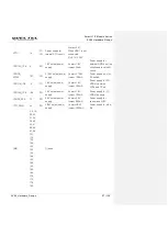
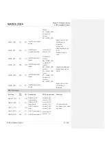
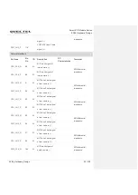
MI2S_2_WS
203
DO I2S word select signal
1.8V power domain.
MI2S_2_DATA0
249
IO
I2S DATA0 signal
1.8V power domain.
MI2S_2_SCK
250
DO I2S serial clock signal
1.8V power domain.
MI2S_2_DATA1
251
IO
I2S DATA1 signal
1.8V power domain.
MI2S_2_MCLK
114
DO I2S main clock signal
1.8V power domain.
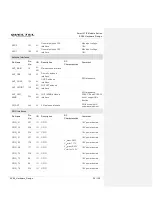
LPI_MI2S_SCLK 212
DO
LPI_I2S serial clock
signal
1.8V power domain.
Cannot be multiplexed
into a general-purpose
GPIO.
LPI_MI2S_WS
156
DO LPI_I2S word select
LPI_MI2S_
DATA0
154
IO
LPI_I2S signal data0
LPI_MI2S_
DATA1
155
IO
LPI_I2S signal data1
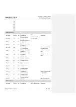
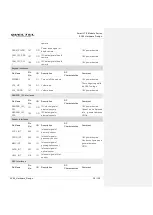
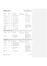
Emergency Download Interface
Pin Name
Pin
No.
I/O
Description
DC
Characteristics
Comment
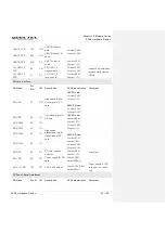
USB_BOOT
57
DI
Force the module to
enter emergency
download mode
Pulled up to
LDO13A_1P8 during
power-up will force the
module to enter
emergency download
mode.
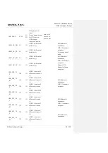
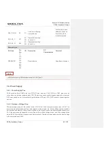
Other Interfaces
Pin Name
Pin
No.
I/O
Description
DC
Characteristics
Comment
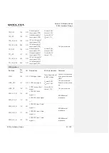
BAT_PLUS
27
AI
Battery voltage detection
differential input (+)
Must be connected.
BAT_MINUS
28
AI
Battery voltage detection
differential input (-)
Must be connected.
BAT_THERM
29
AI
Battery temperature
detection
Internally pulled up.
Externally connected
to GND via a 47KΩ
NTC resistor.
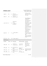
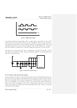
GNSS_PPS_
OUT
202
DO LNA enable control
1.8V power domain;
It should not be pulled
up.

