GSM/GPRS/GNSS Module Series
MC60 Series Hardware Design
MC60_Series_Hardware_Design Confidential / Released 29 / 114
VBAT
C2
C1
+
C3
C4
GND
100uF
100nF
10pF
0603
33pF
0603
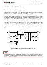
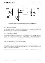
Figure 6: Reference Circuit for the VBAT Input (GSM Part)
3.5.2.2. Decrease Supply Voltage Drop for GNSS Part
Power supply range of GNSS part is from 2.8 to 4.3V. GNSS_VCC
’s maximum average current is 40mA
during GNSS acquisition after power up. So it is important to supply sufficient current and make the power
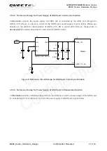
clean and stable. The decouple combination of 10uF and 100nF capacitor is recommended nearby
GNSS_VCC pin. A reference circuit is illustrated in the following figure.
GNSS_VCC
C2
C1
GND
10uF
100nF
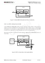
Figure 7: Reference Circuit for the GNSS_VCC Input
Quectel
Confidential

