EL640.480 AG1 Series User’s Manual (020-0350-00B)
9
Interface Information
This dual scan LCD-type video interface provides a low cost, flexible method for
controlling display brightness and power consumption. Many off-the-shelf
chipsets are available for interfacing to flat panel displays. If your application does
not require chip-level integration, there are many vendors that can supply board-
level solutions for serial control, PC104, ISA, and many other interfaces.
Planar Application Note 116 summarizes some of the interfacing options that
have been used in the past with EL VGA displays.
Video Input Signals
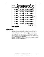
The end of the top line of a frame is marked by S, scan start up signal as shown in
Figure 2. The end of each row of data is marked by CP1 as shown in Figure 2 and
Figure 3.
Input signals UD3—UD0 contain the video data for the upper screen and signals
LD3—LD0 contain the data for the lower screen. For example, four pixels (UD3—
UD0) are sent to row 1 at the same time as four pixels (LD0—LD3) are sent to row
241. This results in eight pixels sent on each cycle of video clock CP2. Pixel
information is supplied from left to right and from top to bottom. Video data for
one row is latched on the fall of CP1 (Figure 4).
S (FRAME)
CP1 (LINE)
UD3 to UD0
LD3 to LD0
frame n- 1
frame n
frame n+ 1
row 240/480
row 1/241
row 1/241
160 CP2 pulses
CP1 (LINE)
UD3 to UD0
LD3 to LD0
First pixels (1...4)
Last pixels (637...640)
240 CP1 pulses
T1
T2
T3
Figure 1. Video Input Timing Diagram.


