background image


EL240.128.45 Operations Manual (020-0345-00C) 

11 

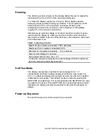
Dimming 

The dimming control circuitry on the display allows the user to adjust the 
luminance from 5 % to 95 % of the maximum brightness. 

To control the display luminance, connect a 50 k

 variable resistor 

between ground and the dimming pin (LUMA). The full resistance of 50 
k

 will result in 95 % of the maximum luminance. Reducing the 

resistance will reduce the luminance, with resistance of 0 

 yielding 

roughly 5 % of the maximum luminance. 

Alternatively an external voltage or current-mode D/A converter may be 
used to dim the display by sinking a maximum of 250 

µ

A for maximum 

dimming from LUMA to ground. When left open, the luminance will remain 
at the maximum level. 

Table 7. Luminance Control. 

Maximum (No resistor connected): 100 % (Default) 
Maximum (50 k 

 resistor connected): 95 % 

Minimum (0 

Ω 

resistor connected):   5 % maximum 

Open Circuit voltage 4 V nominal 
Sink Current 250 

µ

A max, Vin = 0 V 

Luminance values are measured as a percentage of full On Luminance 
(with the external resistor disconnected.) 


Self-Test Mode 

The display incorporates a self-test mode composed of a 1 x 1 
checkerboard and full-on pattern displayed at 240 Hz. Upon power up, 
the 1 x 1 pattern is displayed for several seconds, then the full-on pattern 
is displayed continuously. The self-test mode is entered by leaving the 
SELFTEST pin pulled high. For normal operation the SELFTEST pin must 
be pulled to a logic low. If the SELFTEST pin is pulled high during normal 
operation, the display will enter the self-test mode with the all-pixels-on 
pattern. 


Power-up Sequence 

No special power-up or video sequencing is required. 

Summary of Contents for EL240.128.45 ICEBrite

Page 1: ...EL240 128 45 ICEBrite EL Small Graphics Display USER S MANUAL www planar com...

Page 2: ...Revision Control Date Description August 2000 Document number OM320 00 June 2004 Document number 020 0345 00A September 2005 Document number 020 0345 00B May 2010 Document number 020 0345 00C...

Page 3: ...1 Optical 12 Command Description 12 Required register settings and configuration items 12 Environmental 13 Reliability 13 Safety and EMI Performance 13 Mechanical Characteristics 14 Component Envelope...

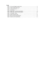
Page 4: ...e 3 Connector Pinouts J1 7 Table 4 Pin Settings 8 Table 5 8080 Video Input Timing Description 9 Table 6 6800 Video Input Timing Description 10 Table 7 Luminance Control 11 Table 8 Optical Characterist...

Page 5: ...individually addressable to clearly display high information content graphics and text Features and Benefits Excellent visual performance High brightness and contrast Wide viewing angle 160 No compen...

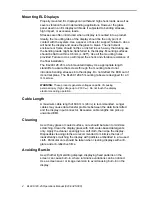
Page 6: ...introduce bending stresses into the display Do not deflect the ECB out of its normal plane The EL240 128 45 mounting tabs were designed for a 3 mm screw WARNING These products generate voltages capabl...

Page 7: ...s manual should be met without exception to ensure the long term reliability of the display Performance characteristics are guaranteed when measured at 25 C with rated input voltage unless otherwise s...

Page 8: ...VI max 0 3 VL 0 3 V Low level input voltage VIL 0 0 2 x VL V HIgh level input voltage except SEL1 VIH 0 5 x VL VL V HIgh level input voltage SEL1 0 8 x VL VL Logic input current IL 10 2000 A Signals W...

Page 9: ...nd connector options J1 Pin 1 Back of display Bottom of display Figure 2 Data Power Connector J1 Table 3 Connector Pinouts J1 Pin Signal Description Pin Signal Description 1 VH Display voltage 2 VH 12...

Page 10: ...n low resets RA8835A must be high or unconnected in normal operation READY Pin 22 OUTPUT When data for Row 128 is written to display drivers this signal goes high While the signal is high it is possib...

Page 11: ...al Symbol Parameter Condition min max unit A0 CS tAH8 Address hold time 10 ns tAW8 Address setup time 0 ns WR RD tCYC System cycle time 550 ns tCC Strobe pulsewidth 120 ns CL 100 pF tDS8 Data setup ti...

Page 12: ...mbol Parameter Condition min max Unit A0 CS tCYC6 System cycle time 550 ns R W tAW6 Address setup time 0 tAH6 Address hold time 0 ns tDS6 Data setup time 100 ns CL 100 pF D0 to D7 tDH6 Data hold time...

Page 13: ...Table 7 Luminance Control Maximum No resistor connected 100 Default Maximum 50 k resistor connected 95 Minimum 0 resistor connected 5 maximum Open Circuit voltage 4 V nominal Sink Current 250 A max Vi...

Page 14: ...ller refer to the Command Description section of the RA8835 manual titled RA8835 Dot Matrix LCD Controller Specification This document is on the RAiO website at http www raio com tw Required register...

Page 15: ...ting non operating 100 g 6 ms duration half sine wave three shocks per surface 6 tested per IEC 68 2 27 Test Ea Thermal Shock 40 C for 30 min room temperature for 3 min then 85 C for 30 min Cycle repe...

Page 16: ...1 height 0 26 0 01 Pixel Pitch millimeters inches horizontal 0 45 0 018 nominal vertical 0 45 0 018 nominal Component Envelope The component envelope shown in Figure 4 illustrates the distance compone...

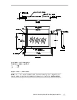
Page 17: ...are millimeters Tolerances unless specified x 0 50 xx 0 25 Figure 5 Display Dimensions Note This is not a controlled version of the mechanical drawing Prior to beginning your design please contact Pla...

Page 18: ...o Seller on a warranty claim and Seller shall pay costs of returning Goods to Buyer The turnaround time on repairs will usually be 30 working days or less Seller accepts no added liability for additio...

Page 19: ...EL240 128 45 Operations Manual 020 0345 00C 17...

Page 20: ...5am 5pm Pacific Time Europe and Asia Pacific Support Olarinluoma 9 P O Box 46 FIN 02201 Espoo Finland Tel 358 9 420 01 Hours M F 7 00am 3pm CET 2010 Planar Systems Inc 10 05 Planar is a registered tra...

Reviews: