background image

69

PDR-W739

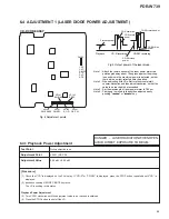
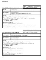
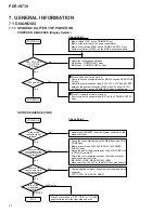
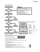
[Procedure]

(1) Press the SYNCHRO button in Stop mode.

Note:  Make sure the unit is in Stop mode.

(2) Check that "OPT" disappears on the FL display.

(3) Press the AUTO SPACE button so that "CDR  04ff34

∗∗

" appears on the FL display.

(4) Press the FINALIZE button for focus-in.

(5) Press the PLAY/PAUSE 

6

 button for CAV-servo spindle kick.

(6) Press the PLAY/PAUSE 

6

 button to close the tracking servo, then set the unit to Playback mode.

(7) Adjust with the REC LEVEL knob until the above adjustment value to be reached is obtained.

Press the REC LEVEL knob to register the adjustment.  Once the adjustment is registered with the REC LEVEL knob, " ERASE " on the

FL display will disappear.

(8) Press the STOP button to stop the unit.

Note:  Adjustment must be done around mid-radius on a disc.

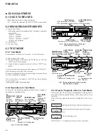
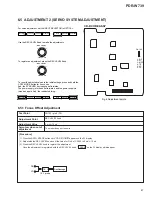
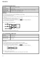
6.5.4 Focus Bias Adjustment

CN102 - pin 1 (RF)

Test Point

Adjustment Point

Adjustment Value

SYNCHRO button, REC LEVEL knob

Adjust until RF jitter is minimal or that the eye pattern of the RF waveform is most open.

Jitter Meter

10:1 probe

or

10 : 1

Oscilloscope

RF

VC

Symptom when out of
adjustment

Sound broken, record characteristics deteriorate

Summary of Contents for PDR-W739

Page 1: ...7 2 PARTS 76 7 2 1 IC 76 7 2 2 DISPLAY 85 7 3 EXPLANATION 87 7 3 1 ERROR CODE 87 8 PANEL FACILITIES AND SPECIFICATIONS 88 T IZK JAN 2000 Printed in Japan COMPACT DISC RECORDER MULTI CD CHANGER Type Model Power Requirement Remarks PDR W739 KUXJ CA AC120V NYXJ AC230V NVXJ AC230V THIS MANUAL IS APPLICABLE TO THE FOLLOWING MODEL S AND TYPE S REC LEVEL CD SELECT COPY START CD CD R COPY MODE CHECK ERASE...

Page 2: ... evident from visual inspection nor the protection afforded by them necessarily can be obtained by using replacement components rated for voltage wattage etc Replacement parts which have these special safety characteristics are identified in this Service Manual Electrical components having such features are identified by marking with a on the schematics and on the parts list in this Service Manual...

Page 3: ...ith the servo mechanism block removed and turned over close viewing of the objective lens with the naked eye will cause exposure to a Class 1 laser beam Additional Laser Caution Refer to page 64 LABEL CHECK CD RECORDER CD PLAYER IMPORTANT THIS PIONEER APPARATUS CONTAINS LASER OF CLASS 1 SERVICING OPERATION OF THE APPARATUS SHOULD BE DONE BY A SPECIALLY INSTRUCTED PERSON LASER DIODE CHARACTERISTICS...

Page 4: ...glish French 1 PACKING PARTS LIST Mark No Description Part No 2 EXPLODED VIEWS AND PARTS LIST NOTES Parts marked by NSP are generally unavailable because they are not in our Master Spare Parts List The mark found on some component parts indicates the importance of the safety factor of the part Therefore when replacing be sure to use parts of identical designation Screws adjacent to mark on the pro...

Page 5: ...ANGER MECHANISM Refer to 2 4 CD R CORE ASSY 1 2 Refer to 2 3 FRONT PANEL SECTION 11 49 47 50 39 23 50 50 50 50 50 50 2 50 8 6 1 NYXJ NVXJ Only NYXJ NVXJ Only KUXJ CA Only NYXJ Only 27 29 50 26 38 25 19 50 31 42 43 18 17 16 18 20 51 5 21 21 22 3 9 4 30 50 50 52 62 62 28 52 24 50 53 50 53 52 56 36 62 58 59 52 37 40 60 61 66 64 63 67 63 65 32 34 35 33 41 44 17 2 2 EXTERIOR SECTION ...

Page 6: ...nger Mechanism AXA7077 11 Supporter L ANG7290 12 Supporter R ANG7291 13 16P FFC 30 PDD1209 14 Connector Assy 6P PDE1308 15 Connector Assy PG11KK E12 NSP 16 Under Base PNA2518 17 Disc Guard PNM1245 18 Insulator PNW2766 19 PCB Supports AEC7132 20 PCB Mold AMR2534 21 PCB Mold AMR2533 NSP 22 Wire Clip VEC1181 NSP 23 Mecha Base C PNB1617 NSP 24 Mecha Base R PNB1616 25 Rear Base See Contrast table 2 26 ...

Page 7: ...12 Self lighted Button PAC1997 13 PLAY Button PAC1979 14 RANDOM Button PAC1996 15 O C Button PAC1982 16 20P FFC 60V PDD1205 17 HEADPHONE Knob PAC1707 18 JOG Knob D508 PAC1939 19 Screw PPZ30P080FMC 20 Screw ABA7009 21 Ceramic Capacitor CKCYB471K50 22 Earth Lead Unit PDF1205 NSP 23 Spacer VEC 244 2 CONTRAST TABLE PDR W739 KUXJ CA NYXJ and NVXJ Types are constructed the same except for the following ...

Page 8: ...33 13 Loading Gear VNL1734 14 Drive Gear VNL1735 15 Drive Cam VNL1736 16 Lock Plate VNL1820 17 Tray Stopper VNL1739 18 Connector Assy PG03KK E37 LOADING A CN501 CD R CORE CN451 19 Screw BBZ26P040FMC 20 Screw Z39 019 21 Loading Motor Assy VXX2505 22 Binder ZCA T18S 23 Clamper Plate VNE2068 24 Bridge VNE2069 25 Clamper VNL1738 26 Screw IPZ26P060FMC 27 32P Flexible Cable 30V PDD1195 CD R Pickup CD R ...

Page 9: ...Disc Table Mark No Description Part No CD R CORE ASSY 2 2 PARTS LIST 2 5 CD R CORE ASSY 2 2 NSP 1 SERVO MECHANISM Assy PWZ3759 2 DC Motor Assy SPINDLE PEA1235 NSP 3 DC Motor CARRIAGE PXM1042 4 Float Rubber A VEB1301 5 Float Rubber B AEB7066 NSP 6 Rack Spring DBH1285 NSP 7 Reflection Sheet PNM1325 8 Servo Base PNW2853 9 Pinion Gear PNW2854 10 Gear A PNW2855 11 Gear B PNW2856 12 Gear C PNW2857 13 Ra...

Page 10: ...13 16 Blue Black 28 44 43 43 22 21 23 24 14 18 15 2 3 5 5 1 7 7 10 9 8 6 No 36 Sub Tray Part Column 2 2 2 2 Gutter 1 Gutter 1 Gutter 1 Boss 1 Gutter 1 1 Gutter Inside Rail 1 Inside Rail 2 Inside Gutter 1 1 Rail 2 Gutter 2 Bottom Gutter 2 Bottom Gutter Whole Left Front Under Gutter 37 45 2 6 3CD MICROCHANGER MECHANISM ...

Page 11: ...140 18 Belt AEB7159 19 Elevator Base ANW7132 20 Tray Guide ANW7150 21 TG Stopper ANW7151 22 TG Spring ABH7175 23 Cam Plate ANW7147 24 Lock Lever ANW7148 25 Float Rubber A Blue AEB7063 26 Float Rubber B Black AEB7066 27 Float Base ANW7130 28 Clamper Holder ANW7152 29 Yoke ANG7257 30 Clamper Magnet AMF7001 31 Clamper SO XNW3007 32 Swing Base ANW7131 33 Main Tray ANW7133 34 Lock Plate ANW7144 35 Lock...

Page 12: ...R SRDR TFDR TRDR FFDR FRDR CDLRCK CDDATA CDBCK 6 10 3 8 15 14 13 16 1 A D A H 76 73 71 68 WRF FE TE RFAC RFWBL IC101 AK8563 RF PROCESSOR LD CONTROL CIRCUIT 58 11 10 29 46 43 39 41 50 IC431 PDK 041A STRATEGY CONTROL 52 19 FG RFDC HF 38 29 34 35 31 32 FCS TRK CN1 7 10 13 16 4 1 3 2 34 35 34 35 CN101 CN452 CN601 PC651 NJL5803K F1 FG Generator 19 17 2872MHz HF FG TE RFWBL 65 67 66 64 6 4 CDLRCK CDBCK ...

Page 13: ...3 1 13 IC1504 HD74HC4053FP CDLRCK CDBCK CDDATA A B 5 XTI IC801 PE8001A PCM1716E D A for output 1 3 2 LINE OUT IC1600 IC1505 HD74HC4053FP CDLRCK CDBCK CDDATA LRCK BCKIN DIN 4 15 14 5 2 12 DALRCK DABCK DADATA 3 1 13 A B 16 13 L R XTI IC701 LC75710NE FL DRIVER 64 63 62 FLD FLCL FLCE V701 FL DISPLAY Key Input REC VOL JOG with Push Button 64 63 62 16 13 6 2 6 2 DACL DACR CN301 CN502 CN501 CN1501 CN1502...

Page 14: ...ELECT UNIT AWU7433 OPERATING 3 ASSY PWZ4067 OPERATING 2 ASSY PWZ4066 3CD MICRO CHANGER MECHANISM ASSY AXA7077 G HEADPHONE ASSY PWZ4071 L P OPERATING 1 ASSY KUXJ CA PWZ4065 NYXJ NVXJ PWZ4073 N O LOADING UNIT AWU7432 MOTOR UNIT AWU7431 F E KUXJ CA AC120V 60Hz NYXJ NVXJ AC230V 50 60Hz AC POWER CORD KUXJ CA ADG7022 NYXJ ADG1154 NVXJ ADG1156 LIVE J1 J2 J1 J2 NEUTRAL AC INLET CN101 J102 J102 J101 J101 P...

Page 15: ... A 5 5 CD R CORE ASSY PYY1279 A C D B LOADING A ASSY PWZ3760 SERVO MECHANISM ASSY PWZ3759 LOADING B ASSY PWZ3761 I OPT I O ASSY PWZ4072 PDD1195 CN601 CN501 CN551 CN101 CN452 CN451 CN453 Note When ordering service parts be sure to refer to EXPLODED VIEWS and PARTS LIST or PCB PARTS LIST ...

Page 16: ...PDR W739 16 A B C D 1 2 3 4 1 2 3 4 A5 5 A2 5 A4 5 A3 5 ATIP DECODER A 1 5 CD R CORE ASSY PYY1279 MECHA CONTROL µCOM BLOCK 3 3 CD R CORE ASSY 1 5 1 5 A ...

Page 17: ...PDR W739 17 A B C D 5 6 7 8 5 6 7 8 MECHA µ COM 8 bit LATCH A4 5 IC303 PYY1196 EEPROM CN301 CN1401 1 2 4 5 7 3 6 8 9 10 11 12 H 1 3 1 5 A ...

Page 18: ...DR W739 18 A B C D 1 2 3 4 1 2 3 4 CD R PICKUP PEA1352 CN1 CN101 7 8 MULTI PLEXER MULTI PLEXER A 2 5 CD R CORE ASSY PYY1279 RF PROCESSOR BLOCK R R R R R R R R 3 4 CD R CORE ASSY 2 5 and CD R PICKUP 2 5 A ...

Page 19: ...PDR W739 19 A B C D 5 6 7 8 5 6 7 8 CN102 4 3 2 1 5 6 RF PROCESSOR A3 5 A5 5 A1 5 A4 5 A3 5 R RF SIGNAL ROUTE AUDIO SIGNAL ROUTE REC R R R R R R R R 2 5 A ...

Page 20: ...PDR W739 20 A B C D 1 2 3 4 1 2 3 4 A2 5 A1 5 A5 5 A2 5 2 3 5 CD R CORE ASSY 3 5 3 5 A ...

Page 21: ...PDR W739 21 A B C D 5 6 7 8 5 6 7 8 1 CDR SERVO AMP MULTI PLEXER A1 5 A4 5 A3 5 A1 5 A 3 5 CD R CORE ASSY PYY1279 SERVO BLOCK 3 5 A ...

Page 22: ...DR W739 22 A B C D 1 2 3 4 1 2 3 4 A 4 5 CD R CORE ASSY PYY1279 DIGITAL BLOCK VCO STRATEGY CONTROL EFM ENCODER IC A3 5 A 2 5 A 2 5 A 1 5 A1 5 18 15 17 16 14 13 R R R R R R R 3 6 CD R CORE ASSY 4 5 4 5 A ...

Page 23: ...7 8 The power supply is shown with the marked box D RAM FS CONVERTER MULTI PLEXER VCO CN501 CN502 A5 5 2 3 1 4 6 7 8 9 10 11 5 12 MULTI PLEXER CN1502 H 2 3 CN1501 H 2 3 R AUDIO SIGNAL ROUTE AUDIO SIGNAL ROUTE REC R R R R EXXTAL 4 5 A ...

Page 24: ...N501 CN601 CN551 J601 S501 LOADING A ASSY PWZ3760 C LOADING B ASSY PWZ3761 D LOADING MOTOR ASSY VXX2505 SERVO MECHANISM ASSY PWZ3759 B CARRIAGE MOTOR ASSY SLIDER PEA1350 DC MOTOR ASSY SPINDLE PEA1235 S601 5ch ACTUATOR DRIVER A 3 5 A2 5 3 1 2 3 7 CD R CORE 5 5 SERVO MECHANISM LOADING A and LOADING B ASSYS 5 5 A B C D ...

Page 25: ...PDR W739 25 A B C D 5 6 7 8 5 6 7 8 The power supply is shown with the marked box CN901 CD DECODER A2 5 A1 5 A4 5 CN33 M 5 4 RF SIGNAL ROUTE AUDIO SIGNAL ROUTE 5 5 A ...

Page 26: ... 0V 5V at MUTE ON Audio Signal Not Output at MUTE OFF Audio Signal Output AMUTE CN501 pin9 5V 0V LRSTD CN501 pin10 5V Note The encircled numbers denote measuring point in the schematic diagram 1 CN301 pin 5 MREQ V 0 2V div 10 1 H 5msec div STOP 2 CN301 pin 6 EN_CE V 0 2V div 10 1 H 5msec div STOP 3 CN301 pin 8 XFUSE V 0 2V div 10 1 H 5msec div STOP 4 CN301 pin 9 MACK V 0 2V div 10 1 H 5msec div ST...

Page 27: ...2 pin 6 FE V 5mV div 10 1 H 2msec div PLAY 5 TP113 RFAC V 0 2V div 10 1 H 0 2µsec div PLAY 6 IC101 pin 22 ATFG V 0 2V div H 20µsec div REC 7 CN101 pin 3 TRK V 0 2V div 10 1 H 5msec div STOP 8 CN101 pin 4 FCS V 0 2V div 10 1 H 5msec div STOP CD R CORE ASSY A2 5 CD R CORE ASSY A3 5 1 TP210 FG V 0 2V div 10 1 H 1msec div PLAY 2 Foot of R212 SPDL V 20mV div H 2msec div PLAY ...

Page 28: ... 17M V 0 2V div 10 1 H 50msec div REC 15 TP502 ODON V 0 2V div 10 1 H 0 1µsec div REC 16 IC431 pin 35 WLDON V 0 2V div 10 1 H 1msec div REC 17 IC431 pin 36 REWLDON V 0 2V div 10 1 H 1msec div REC 5 CN501 pin 12 CL V 0 2V div 10 1 H 0 5µsec div STOP 11 CN501 pin 20 DIN2 V 0 2V div 10 1 H 0 2µsec div REC_Coaxial 18 TP503 W XR V 0 2V div 10 1 H 1msec div REC 1 CN452 pin 2 SL V 0 2V div 10 1 H 5msec d...

Page 29: ...NIT KSM213CCM F CN101 S11B PH K S J102 J102 J101 J101 3 3 H CN1302 3 3 H CN1301 3 3 H CN1101 FOCUS SERVO LOOP LINE F L S S C C F F F T F T T T C C S S L L L TRACKING SERVO LOOP LINE T SPINDLE SERVO LOOP LINE S CARRIAGE SERVO LOOP LINE C LOADING SERVO LOOP LINE L 3 8 MOTOR LOADING SELECT and PICKUP UNITS E F G ...

Page 30: ... 3 H 2 3 H CN701 N 6 7 1 2 5 4 3 NYXJ NVXJ ONLY KUXJ CA ONLY The power supply is shown with the marked box PCB Printing Parts List No No R1463 F7463 R1494 R1499 F7494 F7499 R1438 F7438 R1439 F7439 R1441 F7441 R1461 F7461 3 9 MAIN ASSY 1 3 1 3 H ...

Page 31: ...PDR W739 31 A B C D 5 6 7 8 5 6 7 8 H 1 3 MAIN ASSY KUXJ CA PWX1618 NYXJ NVXJ PWX1619 2 3 H CN301 A 1 5 C964 0 0047 YB 1 3 H ...

Page 32: ...NYXJ NVXJ PWX1619 CN502 A 4 5 CN501 A 4 5 3 3 H 1 3 3 3 H 8 10 11 9 R COPY A R R R R R CDR R CDR CDR CDR CDR C C C C COPY A C C C R COPY A COPY A COPY A COPY A COPY A COPY A COPY COPY COPY COPY A COPY A COPY A COPY A COPY A COPY A COPY A COPY A 3 10 MAIN ASSY 2 3 2 3 H ...

Page 33: ...GNAL at CDR side CDR COPY SIGNAL COPY COPY ANALOG SIGNAL COPY A COPY A COPY A R COPY A R COPY A R COPY A R COPY A R COPY A R COPY A C C C R COPY A R COPY A COPY A AUDIO SIGNAL for LINE OUT REC SIGNAL of External Analog Input R J1690 L KUXJ CA NYXJ NVXJ The power supply is shown with the marked box OTL1040 2 3 H ...

Page 34: ...PDR W739 34 A B C D 1 2 3 4 1 2 3 4 H 3 3 MAIN ASSY KUXJ CA PWX1618 NYXJ NVXJ PWX1619 CN101 TO PICKUP UNIT E 16 C1332 0 001 C1344 0 001 YB YB KUXJ CA TYPE ONLY KUXJ CA TYPE ONLY 3 11 MAIN ASSY 3 3 3 3 H ...

Page 35: ...PDR W739 35 A B C D 5 6 7 8 5 6 7 8 1 3 H 2 3 H 2 3 H AUDIO SIGNAL ROUTE 3 CD C C RF SIGNAL ROUTE 17 19 18 20 21 24 23 22 The power supply is shown with the marked box 3 3 H ...

Page 36: ... 0 2µsec div CD CD R Double speed interrnal analog copy 12 IC801 pin 5 XTI V 2V div H 50nsec div CD CD R Double speed copy 13 IC801 pin 27 DAC CLK V 2V div H 5msec div CD PLAY at 3CD side 10 IC803 pin 3 BCK IN V 2V div H 0 2µsec div CD CD R Double speed interrnal analog copy 11 IC803 pin 5 XTI V 2V div H 50nsec div CD PLAY at 3CD side 14 IC801 pin 26 DAC data V 2V div H 5msec div CD PLAY at 3CD si...

Page 37: ...v CD PLAY at 3CD side 23 IC1201 pin 65 LRCK V 2V div H 5µsec div CD PLAY at 3CD side 24 IC1201 pin 64 DOUT V 2V div H 0 2µsec div CD PLAY at 3CD side MAIN ASSY H3 3 IC1201 pin 25 MDP V 2V div H 5µsec div CD PLAY at 3CD side 1 IC1201 pin 25 MDP V 2V div H 5µsec div CD CD R Double speed copy IC1201 pin 6 CD DCLK V 2V div H 2msec div CD PLAY at 3CD side IC1201 pin 4 CD DATA V 2V div H 0 5msec div CD ...

Page 38: ...TRANS ASSY KUXJ CA PWZ4070 NYXJ NVXJ PWZ4087 PRIMARY ASSY KUXJ CA PWZ4069 NYXJ NVXJ PWZ4084 J HEADPHONE ASSY PWZ4071 L POWER TRANSFORMER KUXJ CA PTT1363 NYXJ NVXJ PTT1364 AC INLET KUXJ CA AKP7032 NYXJ NVXJ AKP1046 AC IN KUXJ CA KUXJ CA NVXJ NYXJ NVXJ NYXJ 1A 125V REK1075 3 12 OPT I O TRANS PRIMARY HEADPHONE and POWER SUPPLY ASSYS L M I J K ...

Page 39: ...Y A COPY A R COPY A R COPY A R COPY A R R CAUTION FOR CONTINUED PROTECTION AGAINST RISK OF FIRE REPLACE ONLY WITH SAME TYPE NO 4911 25 FOR IC30 IC32 AND IC37 491 750 FOR IC33 IC35 AND IC38 MFD BY LITTELFUSE INC NOTE FOR FUSE REPLACEMENT FOR CONTINUED PROTECTION AGAINST RISK OF FIRE REPLACE WITH SAME TYPE AND RATINGS ONLY CAUTION The power supply is shown with the marked box M ...

Page 40: ...3 4 1 2 3 4 N OPERATING 1 ASSY KUXJ CA PWZ4065 NYXJ NVXJ PWZ4073 The power supply is shown with the marked box PCB Printing Parts List No No R733 F8733 R734 F8734 R735 F8735 3 13 OPERATING 1 OPERATING 2 and OPERATING 3 ASSYS N ...

Page 41: ...708 41 REV OPERATING 3 ASSY S709 0 OPEN CLOSE 3 S710 0 OPEN CLOSE 2 S730 0 OPEN CLOSE 1 S719 CD SELECT 2 S720 CD SELECT 1 S721 7 STOP S722 DISP S723 FF S724 6 PLAY PAUSE S725 41 REV S726 SYNCHRO S727 OPEN CLOSE S728 REC REC MUTE OPERATING 1 ASSY S711 AUTO SPACE S712 INPUT S713 FINALIZE S714 ERASE S715 CHECK S716 COPY MODE S717 COPY START CD CD R S718 CD SELECT 3 N O P ...

Page 42: ...ic diagrams is shown below 3 The parts mounted on this PCB include all necessary parts for several destinations For further information for respective destinations be sure to check with the schematic diagram 4 View point of PCB diagrams Symbol In PCB Diagrams Symbol In Schematic Diagrams Part Name B C E D D G G S S B C E B C E D G S B C E B C E B C E Transistor Transistor with resistor Field effec...

Page 43: ...ANISM LOADING A and LOADING B ASSYS D C B SIDE A SIDE B PNP1471 B CN452 A CN451 A CN453 A SERVO MECHANISM ASSY B LOADING A ASSY C LOADING B ASSY D LOADING B ASSY D LOADING A ASSY C SERVO MECHANISM ASSY B M M M CARRIAGE MOTOR SPINDLE MOTOR LOADING MOTOR ...

Page 44: ...303 Q402 Q401 IC401 IC501 IC507 Q304 IC506 IC352 Q451 Q452 IC451 IC201 IC502 IC509 Q203 Q101 Q204 IC251 IC254 Q201 IC101 Q142 IC562 IC431 IC432 VR161 VR141 VR162 VR163 VR101 CN33 M CD R CORE ASSY A CN1401 H CN1502 H CN1501 H To CD R PICKUP CN601 B CN501 C CN551 D SIDE A This diagram has four layers In the two middle layers mainly Vcc and GND are Connected ...

Page 45: ...D 1 2 3 4 1 2 3 4 A PNP1475 B Q551 Q202 IC255 IC505 IC508 IC181 Q102 IC561 IC141 IC143 IC142 IC161 Q103 Q141 CD R CORE ASSY A SIDE B This diagram has four layers In the two middle layers mainly Vcc and GND are Connected ...

Page 46: ...PDR W739 46 A B C D 1 2 3 4 1 2 3 4 4 4 MAIN ASSYS H Q1101 IC1101 IC1302 IC1301 IC801 IC1402 Q1403 MAIN ASSY H CN3 M CD MECHA CN101 E CN701 N J1690 L CD MECHA ...

Page 47: ...PDR W739 47 A B C D 5 6 7 8 5 6 7 8 H PNP1472 A IC1509 IC803 IC1507 IC1508 IC1506 IC801 IC1201 IC1401 CN30 M CN301 A CN502 A CN501 A SIDE A ...

Page 48: ...PDR W739 48 A B C D 1 2 3 4 1 2 3 4 H IC1505 IC1503 Q1501 IC1504 IC1502 MAIN ASSY H ...

Page 49: ...PDR W739 49 A B C D 5 6 7 8 5 6 7 8 H PNP1472 A SIDE B ...

Page 50: ... 50 A B C D 1 2 3 4 1 2 3 4 PNP1473 A IC1650 IC1652 IC1651 IC1600 IC1630 IC30 IC31 IC40 IC33 IC34 IC35 IC37 IC39 IC36 IC38 IC32 CN600 I POWER SUPPLY ASSY M CN901 A CN801 H CN10 J SIDE A M 4 5 POWER SUPPLY ASSY ...

Page 51: ...PDR W739 51 A B C D 5 6 7 8 5 6 7 8 M PNP1473 A Q1650 Q1654 Q1690 Q1653 Q1651 Q1601 Q1600 Q1602 Q1652 POWER SUPPLY ASSY M SIDE B ...

Page 52: ...PDR W739 52 A B C D 1 2 3 4 1 2 3 4 4 6 OPT I O TRANS and PRIMARY ASSYS J I K PNP1473 A OPT I O ASSY I PRIMARY ASSY K TRANS ASSY J CN31 H J33 H SIDE A AC IN ...

Page 53: ...PDR W739 53 A B C D 1 2 3 4 1 2 3 4 K J I PNP1473 A OPT I O ASSY I PRIMARY ASSY K TRANS ASSY J SIDE B Q651 Q651 ...

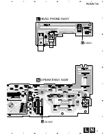
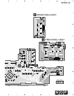
Page 54: ...PDR W739 54 A B C D 1 2 3 4 1 2 3 4 4 7 HEAD PHONE OPERATING1 OPERATING2 and OPERATING3 ASSY O N P PNP1473 A OPERATING3 ASSY P OPERATING2 ASSY O SIDE A ...

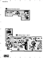
Page 55: ...PDR W739 55 A B C D 5 6 7 8 5 6 7 8 N L HEAD PHONE ASSY L OPERATING1 ASSY N CN802 H CN1402 H ...

Page 56: ...PDR W739 56 A B C D 1 2 3 4 1 2 3 4 N L HEAD PHONE ASSY L OPERATING1 ASSY N Q708 IC701 ...

Page 57: ...PDR W739 57 A B C D 5 6 7 8 5 6 7 8 P O N PNP1473 A OPERATING3 ASSY P OPERATING2 ASSY O SIDE B IC701 Q701 Q704 Q707 Q706 Q705 ...

Page 58: ...NJM2137M IC251 NJU7016M IC201 PA9007A IC507 PCX1026 IC431 PD9020A IC351 PDJ014A IC301 PE5147B IC932 PST994C IC505 TC74HC157AF IC362 TC7S00F IC363 IC562 TC7S04F IC305 IC509 TC7S08F IC361 IC364 TC7S14F IC510 TC7S32F IC506 TC7SU04F IC302 TK11041M 1 Q452 2SK209 Q102 DTA114TK Q204 Q401 Q402 DTA124EK Q551 DTA143EK Q101 Q142 Q201 Q203 DTC114TK Q103 Q141 Q301 Q304 DTC124EK D101 D182 D201 D302 1SS355 D321 ...

Page 59: ...C119 C204 C468 C469 CKSQYB681K50 C463 C464 CKSQYB682K50 C205 CKSQYB683K25 C133 C144 C153 C254 C303 CKSQYF103Z50 C322 C362 C416 C433 C519 CKSQYF103Z50 C521 C555 C561 C562 CKSQYF103Z50 C568 C569 C905 CKSQYF103Z50 C106 C108 C111 C120 C123 CKSQYF104Z25 C125 C129 C132 C143 C152 CKSQYF104Z25 C154 C158 C161 C202 C210 CKSQYF104Z25 C214 C217 C255 C260 C262 CKSQYF104Z25 C301 C302 C306 C309 C310 CKSQYF104Z25...

Page 60: ...C7902 C7903 CCSQCH101J50 C814 C816 C929 C939 CCSQCH101J50 C1503 CCSQCH102J50 C1121 C1505 CCSQCH220J50 C1239 C1246 CCSQCH221J50 C1247 C933 C969 CCSQCH471J50 C1504 CCSQCH7R0D50 C1324 C1343 CEJA100M16 C1101 C1108 C1201 C1203 C1233 CEJA101M10 C1242 C1249 C1401 C1407 C1507 CEJA101M10 C1513 CEJA101M10 C1321 CEJA101M16 C909 C910 CEJA220M50 C801 C808 C822 C867 C868 CEJA221M6R3 C899 CEJA221M6R3 C812 C813 C...

Page 61: ...NK OUT GP1F32T JA600 OPTICAL RECEIV MOD GP1F37R CN600 6P SOCKET KP200TA6L TRANS ASSY Although PWZ4087 and PWZ4070 are different in part number they consist of the same components PARTS LIST FOR PWZ4070 CAPACITORS C10 C25 CKSQYF103Z50 PRIMARY ASSY 1 CONTRAST TABLE PWZ4084 and PWZ4069 are constructed the same except for the following 2 PARTS LIST FOR PWZ4069 SWITCHES AND RELAYS S1 RSA1001 COILS AND ...

Page 62: ... B ANH1021 CN33 KR CONNECTOR B6B PH K S J33 JUMPER WIRE 10P D20PYY1015E CN31 6P PLUG KM200TA6 JA1600 4P PIN JACK PKB1016 JA1680 JACK 12V PKN1004 KN30 KN33 EARTH METAL FITTING VNF1084 OPERATING1 ASSY 1 CONTRAST TABLE PWZ4073 and PWZ4065 are constructed the same except for the following 2 PARTS LIST FOR PWZ4065 SEMICONDUCTORS IC701 LC75710NE Q705 Q707 2SC2412K Q701 Q704 Q708 DTC143EK D701 D706 SLR 3...

Page 63: ...E Spindle motor START Spindle servo CLOSE Tracking servo CLOSE CLOSE OPEN Tracking servo inwards outwards Pickup Move PLAY PAUSE 1 2 PLAY BACK SPEED CD CD R TEST MODE CD TEST MODE CD TEST 2 CD R TEST MODE CDR 00000000 POWER OFF POWER ON POWER OFF _ ON POWER OFF 3 CD 7 7 CD R POWER OFF _ ON POWER ON 3 CD 7 7 CD R PLAY MODE CD TEST MODE NOTE There is no information to be shown in this CD adjustment ...

Page 64: ...DISP 6 7 0 0 0 4 1 DISP 6 7 COMPACT DISC DIGITAL RECORDER 0 COMPACT DISC RECORDER MULTI CD CHANGER CD R CONTROL CD R LD emitting ANA adjustment of LD power OPT adjustment of servo system LD not emitting Switching CD CD R and CD RW Fig 2 During adjustment of LD power Input selector analog CD R Stop CD R LD emitting Focus Servo Close Fig 3 During adjustment of servo system Input selector optical CD ...

Page 65: ...e CD R record power CD RW record power CD RW bias power CD RW recording Fig 5 Output power of the laser diode CD RW erase power Note 1 Attach the remote sensor of the laser power meter to a point angled away about 10 degrees against the pickup lens and where the maximum power is detected so that there will be no light reflected onto the pickup Note 2 When adjusting with VRs first turn them complet...

Page 66: ...ent value of VR163 Procedure 1 Turn VR141 VR161 and VR164 completely counterclockwise to set their power output to minimum 2 Press the ERASE button twice so that CD RW appears on the FL display If the indication is CD or CD R press the ERASE button repeatedly until CD RW appears on the FL display 3 Press continuing the REC REC MUTE button twice The LD is emitting in this status Adjustment of BIAS ...

Page 67: ... LEVEL knob For servo adjustment set the INPUT SELECTOR to OPTICAL Use the REC LEVEL Knob to make the adjustments To reset the adjusted values to the initial settings press and hold the COPY MODE button for 4 seconds And the SYNCHRO key is pushed afterwards The power supply is turned off afterwards and the power supply is turned on again And the readjusted thing To register an adjustment press the...

Page 68: ...ment Value REC LEVEL knob Adjust until the value of the output signals from pin 4 TE and pin 3 MPP of CN102 are the same or the differential output of these signals is minimal Procedure 1 Press the AUTO SPACE button so that CDR 03fff6 appears on the FL display 2 Adjust with the REC LEVEL knob until the above adjustment value to be reached is obtained 3 Press the REC LEVEL knob to register the adju...

Page 69: ...knob until the above adjustment value to be reached is obtained Press the REC LEVEL knob to register the adjustment Once the adjustment is registered with the REC LEVEL knob ERASE on the FL display will disappear 8 Press the STOP button to stop the unit Note Adjustment must be done around mid radius on a disc 6 5 4 Focus Bias Adjustment CN102 pin 1 RF Test Point Adjustment Point Adjustment Value S...

Page 70: ...ller and mechanism controller MSI MSO MSCK MASK MREQ LREQ Mode controller IC1401 on the MAIN Assy breaks down When FL does not turn on at all Check the connection between the MAIN Assy and OPERATING 1 Assy Check the communication lines FLDI FLCL FLCE and FLRST between the system controller IC1402 and FL driver IC701 FL Driver IC701 on the OPERATING1 Assy breaks down Check Point POWER ON SEQUENCE D...

Page 71: ... pin 71 CLAMP SW pin 79 HOME SW pin 80 Mechanism SW logic at HOME position SELINIT SW L SEL SW L OPEN SW H CLOSE SW L CLAMP SW H HOME SW L Initialization Sequence at POWER ON of 3CD MICRO CHANGER MECHANISM Setting the initial condition for shipping Setting the initial operating condition The factory default settings shall be as above For reason that this product memorizes the condition of above it...

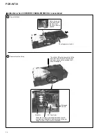
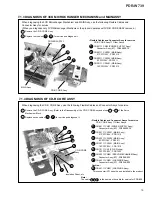
Page 72: ...CN451 Remove connectors CN452 CN101 CN1501 CN1502 CN1401 VR164 VR161 VR141 VR162 VR163 VR101 CD R CORE Assy Bonnet Tray Panel C Tray Panel R 6 5 3 2 5 5 2 2 4 4 2 8 2 9 4 3 8 2 5 2 2 3 1 4 3 5 2 Recorder section OPEN CLOSE 1 Diagnosis of CD R CORE Assy Servo Mechanism Block Drive Gear Front 6 Tray CD R CORE Assy Shield Plate 7 5 10 11 3 Stopper Servo Mechanism Block Shield Case Bonnet 7 1 2 DISASS...

Page 73: ...13 3CD MICROCHANGER MECHA SUB Tray x 3 Hook x2 is removed and the elevator the elevator cover the gear shaft and the loading gear are removed A sub tray becomes free The Hook is removed The bottom of a main tray is lifted Hook take off Main Tray Hook Mecha Base Float Base Swing Base Clamper Holder PICKUP UNIT Blue Black ...

Page 74: ...the home lever is opened The stopper arm is shut The stick of Ø3 plus driver etc of 0 is inserted in the hole of sub three trays and main trays and the position of all trays is arranged Extended Gear B EV Cam Gear Elevator When the elevator is installed Extended Gear B is turned and the ditch in the Elevator and the gear flange of the EV Cam Gear are matched ...

Page 75: ... 8P FFC 30V PDD1211 1 2 3 CN301 CN1401 MAIN Assy 15P FFC 30V PDD1212 4 CN101 CN1 CD R Pickup 32P FFC 30V PDD1202 5 CN452 CN601 SERVO MECHANISM Assy Connector Assy 9P PG09KK E35 6 CN453 CN501 LOADING B Assy Connector Assy 2P PG02KK E35 7 CN451 CN501 LOADING A Assy 8 1 10 CD R CORE Assy Other Assys 1 2 3 4 5 6 7 8 7 1 4 DIAGNOSIS OF CD R CORE ASSY 7 1 3 DIAGNOSIS OF 3CD MICROCHANGER MECHANISM and MA...

Page 76: ...tage setting pin 7 OUT2 Motor output pin 8 GND GND pin Pin Connection Top view Logic table of Input Output Pin Function 5 6 7 8 4 3 2 1 SW CONTROL V B INPUT B INPUT OUTPUT 1 A INPUT 2 A INPUT 3 V 4 8 7 6 5 The information shown in the list is basic information and may not correspond exactly to that shown in the schematic diagrams BA6417F MAIN ASSY IC1302 Motor Drive IC Pin Connection Top view 7 2 ...

Page 77: ...c n e u q e r f h g i H 6 2 P M A D O M I w o L H p a l r e v o y c n e u q e r f h g i h f o g n i t t e s e d u t i l p m A 7 2 1 T 3 I I t u p t u o R X W f o l o r t n o c h t d i w e s l u p l a n g i s t i p T 3 8 2 2 T 3 I 9 2 1 T N I t u p t u o R X W f o g n i t t e s h t g n e l t i P 0 3 D D V y l p p u s r e w o P 1 3 D N G d n u o r G 2 3 2 T N I t u p t u o R X W f o g n i t t e s h ...

Page 78: ...L 7 1 5 0 P C S X E X O L 5 8 5 9 8 C L f o t u p t u o e l b a n e c n y s l a n r e t x E 8 1 6 0 P C N Y S A X O L c n y s e m a r f P I T A 9 1 7 0 P E C N E X I O d e s u t o n t a t r o p t u p n I o t t e S H 5 8 5 9 8 C L f o t u p t u o e l b a n e l a i r e S 0 2 K A D L H Q R F E R X 7 6 P 5 0 3 P T O s t u p t u o p o o L n i a M r e l l o r t n o C E D O M 1 2 Q R D L H T I A W X 6 6 ...

Page 79: ... P B F R A I F R k c a b y a l P f o e p o l e v n e e d i s r e w o l f o t u p n i D A 9 5 3 I N A 3 7 P P M E T A I r o s n e s e r u t a r e p m e t f o t u p n i D A 0 6 4 I N A 4 7 P C P O F R A I t u p n i D A T U O X P M C P O F R 1 6 5 I N A 5 7 P T U O A A I t u p n i D A T U O A 2 6 6 I N A 6 7 P Y A R T A I P M A L C N E P O n o i t i s o p g n i d a o l f o t u p n i D A 3 6 7 I N A 7...

Page 80: ...c l a i r e S I S L d n a r e l l o r t n o c 6 5 4 2 1 P 7 1 T E S E R T E S E R S I t u p n i t e s e r r e l l o r t n o c e d o M 7 5 3 2 1 P 8 1 4 7 P O t u p t u o L d e s u t o N 8 5 2 2 1 P 9 1 3 7 P O 9 5 1 2 1 P 0 2 S S V A D N G D N G o t t c e n n o C 0 6 0 2 1 P 1 2 7 1 P E S U F X O n o i t a c i n u m m o c l a i r e s e h t e s u g n i r u D 5 8 5 9 8 C L d n a r e l l o r t n o c ...

Page 81: ... m o c r e d o c e d D C r o f t u p t u o k c o l c l a i r e S 2 2 0 8 P T A L X D C O d n a m m o c r e d o c e d D C r o f t u p t u o h c t a L 3 2 7 7 P A T A D D C O d n a m m o c r e d o c e d D C r o f t u p t u o a t a d l a i r e S 4 2 6 7 P K L C S D C O r e d o c e d D C f o t u o d a e r l a i r e s r o f t u p t u o k c o l c l a i r e S 5 2 5 7 P O s t u p t u o L d e s u t o N 6 2...

Page 82: ... d l a m r o N d e e p s 6 5 6 3 P O s t u p t u o L d e s u t o N 7 5 5 3 P O 8 5 4 3 P K C A D M O h c t i w s n o i t a r e p o m e t s y S 9 5 3 3 P 4 W S O 0 6 2 3 P 3 W S O 1 6 1 3 P 2 W S O 2 6 C C V C C V D D V o t t c e n n o C 3 6 0 3 P 1 W S O h c t i w s n o i t a r e p o m e t s y S 4 6 S S V S S V I D N G o t t c e n n o C 5 6 7 2 P S E T U M A O e t u m t u p t u o T U O E N I L 6 6...

Page 83: ...D A y e K 4 9 2 N A 2 D A Y E K I 5 9 1 N A 3 D A Y E K I 6 9 S S V A S S V I D N G o t t c e n n o C 7 9 0 N A 4 D A Y E K I D N G o t t c e n n o c n w o d l l u p d e s u t o N t u p n i D A y e K 8 9 F E R V C C V I D D V o t t c e n n o C 9 9 C C V A C C V I 0 0 1 7 9 P T S R L F O r e v i r d L F r o f t u p t u o t e s e R SW1 SW2 SW3 SW4 MDACK 33 16C 2XSEL ADPD1 DUB XVCO PLAY at CD side H ...

Page 84: ...B S M d n a t n e m e l p m o c s 2 s a s t u p t u o a t a D t u p t u o a t a d l a i r e S 0 1 K C R L I k c o l c s f s t u p n I t u p n i k c o l c l e n n a h c R L 1 1 K L C M I t u p n i k c o l c r e t s a M 2 1 K L C S I K L C S f o e g d e g n i l l a f t a s t u p t u o a t a d D A t u p n i k c o l c a t a d l a i r e S 3 1 N D P I n o d e n r u t s i r e w o p n e h w e c n o t e s ...

Page 85: ...P12 P11 P10 P9 P8 P7 P6 P5 40 41 42 43 44 45 46 47 48 49 50 51 52 P4 P3 P2 P1 15G 14G 13G 12G 11G 10G 9G 8G 7G Pin No 53 54 55 56 57 58 59 60 61 62 Assignment 6G 5G 4G 3G 2G 1G NP NP F2 F2 Note 2G to 13G 1 F1 F2 Filament 2 NP No pin 3 DL Datum Line 4 1G to 15G Grid 1 2 2 2 3 1 4 2 5 2 1 1 2 1 3 1 4 1 5 1 1 3 2 3 3 2 4 3 5 3 1 4 2 4 3 3 4 4 5 4 col col Dp S1 1 5 2 5 3 4 4 5 5 5 1 6 2 6 3 5 4 6 5 6 ...

Page 86: ...86 PDR W739 ...
Page 87: ... The optimum recording power cannot be obtained Trouble in RF detection Defective laser diode Trouble in RF detection Defective RFT RFB circuit Recording power is not sufficient Improper soldering pattern short Trouble with power supply Unable to read ATIP or subcode IC201 PA9007A IC101 AK8563 IC363 TC7S04F IC364 TC7S14F F The unit stops during playback or recording Defective pickup Unable to focu...

Page 88: ... playback DISPLAY Use to switch the CD display mode 6 Press to play a disc or pause a disc that s already playing press again to restart play back 7 Press to stop playback 11 RANDOM Start random track disc playback 12 PHONES LEVEL Plug in a pair of head phones Adjust the volume using the level control 13 PLAY MODE Set the play mode to play one disc all discs in the changer or all discs in both the...

Page 89: ...ard playback 4 Skip back forward tracks 3 Numeric and function buttons Number buttons Use to select track num bers 10 0 Use to input 10 or 0 10 Use to enter track numbers greater than 10 RANDOM Start random track disc playback REPEAT Set the repeat mode FADER Fade in or out during playback or recording CD R only PROGRAM Program the playback track order CHECK Check the tracks of a programmed playli...

Page 90: ...rding level is on DIG ANA Indicates whether internal record ing is via a digital or analog link ANA OPT COAX Indicates the current input analog optical or coaxial AUTO SPACE Lights when automatic track spacing is on in program copy mode ALC Lights when automatic analog level control is on 4 COPY X1 X2 Lights when copying disc s tracks from the CD changer and indicates whether single or double spee...

Page 91: ...harmonic distortion 0 005 Output voltage 2 0 V Wow flutter Less than measurement limit 0 001 W PEAK EIAJ Number of channels 2 channels stereo Coaxial output 0 5 Vpp 20 75 Ω Optical output 15 to 21 dBm wavelength 660 nm Frequency deflection Level 2 standard mode Recording specification values are for the LINE input analog 3 Input jacks Optical digital input jack Coaxial digital input jack Audio LIN...

Reviews: