background image

46

PDP-503PE, PDP-503PU

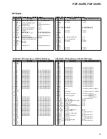
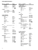
Mark   No.       Description                      Part No.

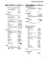
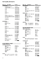
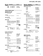
Mark   No.       Description                      Part No.

LIST OF ASSEMBLIES

NSP

SCAN FUKUGO ASSY

AWV1898

NSP

     SCAN (A) ASSY

AWZ6617

NSP

     SCAN (B) ASSY

AWZ6616

NSP

     X CONNECTOR (A) ASSY

AWZ6618

NSP

     X CONNECTOR (B) ASSY

AWZ6619

NSP

     BRIDGE A ASSY

AWZ6620

NSP

     BRIDGE B ASSY

AWZ6621

NSP

     BRIDGE C ASSY

AWZ6622

NSP

     BRIDGE D ASSY

AWZ6623

NSP

     CLAMP A ASSY

AWZ6650

NSP

     CLAMP B ASSY

AWZ6651

NSP

     CLAMP C ASSY

AWZ6652

NSP

     CLAMP D ASSY

AWZ6653

ADDRESS FUKUGO ASSY

AWV1900

NSP

     ADR CONNECT A ASSY

AWZ6626

NSP

     ADR CONNECT B ASSY

AWZ6627

NSP

     ADR CONNECT C ASSY

AWZ6628

NSP

     ADR CONNECT D ASSY

AWZ6629

     ADR RESONANCE ASSY

AWZ6691

X DRIVE ASSY

AWV1901

HD Y DRIVE ASSY

AWV1925

     Y DRIVE ASSY

AWZ6645

     SUB ADDRESS A ASSY

AWZ6689

     SUB ADDRESS B ASSY

AWZ6690

DIGITAL VIDEO ASSY

AWV1903

NSP

HD FUKUGO ASSY

AWV1923

     MR INTERFACE ASSY

AWZ6654

     LED ASSY

AWZ6655

     FRONT KEY ASSY

AWZ6656

     FRONT KEY CONN ASSY

AWZ6657

     IR (P) ASSY

AWZ6658

     THERMAL SENSOR ASSY

AWZ6660

NSP

HD AUDIO ASSY

AWV1935

     AUDIO AMP ASSY

AWZ6687

     SP TERMINAL ASSY

AWZ6688

V MID CLAMP ASSY

AWV1934

SCAN (A) ASSY

SEMICONDUCTORS

IC6001-IC6006

SN755860PJ

CAPACITORS

C6001,C6002,C6011,C6012

ACG1088

(0.1

µ

F/250V)

C6021,C6022,C6031,C6032

ACG1088

(0.1

µ

F/250V)

C6041,C6042,C6051,C6052

ACG1088

(0.1

µ

F/250V)

C6004,C6005,C6009,C6013,C6015

CCSRCH151J50

C6026,C6027,C6038,C6040,C6044

CCSRCH151J50

C6048,C6054,C6058,C6059

CCSRCH151J50

C6007,C6008,C6014,C6019,C6025

CCSRCH181J50

C6028,C6035,C6039,C6046,C6047

CCSRCH181J50

C6056,C6057

CCSRCH181J50

C6003,C6006,C6017,C6018,C6020

CCSRCH390J50

C6023,C6024,C6029,C6033,C6034

CCSRCH390J50

C6037,C6043,C6045,C6049,C6053

CCSRCH390J50

C6055,C6060,C6062-C6066

CCSRCH390J50

C6010,C6016,C6030,C6036,C6050

CKSRYF104Z16

C6061

CKSRYF104Z16

RESISTORS

R6007,R6012,R6021,R6028,R6032

RAB4C221J

R6040

RAB4C221J

Other Resistors

RS1/16S

J

OTHERS

CN6001

15P CONNECTOR

AKP1218

K6001,K6012,K6018,K6025,K6031

AKX9002

TEST PIN

K6038,K6044   TEST PIN

AKX9002

SCAN (B) ASSY

SEMICONDUCTORS

IC6201-IC6206

SN755860PJ

CAPACITORS

C6201,C6202,C6212,C6213

ACG1088

(0.1

µ

F/250V)

C6222,C6223,C6232,C6233

ACG1088

(0.1

µ

F/250V)

C6242,C6243,C6252,C6253

ACG1088

(0.1

µ

F/250V)

Mark   No.       Description                      Part No.

Mark   No.       Description                      Part No.

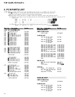
5. PCB PARTS LIST

NOTES:

Parts marked by "NSP" are generally unavailable because they are not in our Master Spare Parts List.

The 

 mark found on some component parts indicates the importance of the safety factor of the part.

Therefore,  when replacing, be sure to use parts of identical designation.

When ordering resistors, first convert  resistance values into code form as shown in the following examples.
 Ex.1 When there are 2 effective digits (any digit apart from 0), such as 560 ohm and 47k ohm (tolerance is shown by J=5%,
          and K=10%).

560 

56 

× 

10

1

561 ........................................................ RD1/4PU 

5


6


1

 J

47k 

47 

× 

10

3

473 ........................................................ RD1/4PU 

4


7


3

 J

0.5 

R50 ..................................................................................... RN2H 

R


5


0

 K

1R0 ..................................................................................... RS1P 

1


R


0

 K

 Ex.2 When there are 3 effective digits (such as in high precision metal film resistors).

5.62k 

Ω →

562 

× 

10

1

5621 ...................................................... RN1/4PC 

5


6


2


1

 F

Summary of Contents for PDP-503PE

Page 1: ...HARGE from the electromaniacs com community You are free to distribute this file to other persons who needs it but without of charge Also on http electromaniacs com you can find thousands of service manuals schematics free of charge ...

Page 2: ...s refer to Important symbols for good services THIS MANUAL IS APPLICABLE TO THE FOLLOWING MODEL S AND TYPE S This Service Manual should be used together with the following manual s Component System Service Manual Remaks Plasma Display System PDP 503HDE Media Receiver PDP R03E PDP R03E ARP3110 PDP R03U ARP3113 Plasma Display PDP 503PE PDP 5030HD PDP R03U PDP 503PU ARP3107 ARP3108 This service manua...

Page 3: ...t and compartment covershields isolation resistor capacitor etc 3 When service is required observe the original lead dress Extra precaution should be taken to assure correct lead dress in the high voltage circuitry area 4 Always use the manufacture s replacement components Especially critical components as indicated on the circuit diagram should not be replaced by other manufacture s Furthermore w...

Page 4: ...ent measured must not exceed 0 5mA ANY MEASUREMENTS NOT WITHIN THE LIMITS OUTLINED ABOVE ARE INDICATIVE OF A POTENTIAL SHOCK HAZARD AND MUST BE CORRECTED BEFORE RETURNING THE SET TO THE CUSTOMER PRODUCT SAFETY NOTICE Many electrical and mechanical parts in PIONEER set have special safety related characteristics These are often not evident from visual inspection nor the protection afforded by them ...

Page 5: ...e of the SW POWER SUPPLY Module CHARGED SECTION AND HIGH VOLTAGE GENERATING POINT 7 High Voltage Generating Point The places where voltage is 100V or more except for the charged places described above If the places are touched there is a risk of electric shock 1 SW POWER SUPPLY Module 225V 2 X DRIVE Assy 300V to 225V 3 Y DRIVE Assy 355V 4 SCAN A Assy 355V 5 SCAN B Assy 355V 6 X CONNECTOR A Assy 30...

Page 6: ...icants glues and replacement parts Appropriately applying grease or glue can maintain the product performances But improper lubrication or applying glue may lead to failures or troubles in the product By following the instructions in this manual be sure to apply the prescribed grease or glue to proper portions by the appropriate amount For replacement parts or tools the prescribed ones should be u...

Page 7: ... 30 For SCHEMATIC DIAGRAM refer to ARP3108 4 PCB CONNECTION DIAGRAM Refer to ARP3108 5 PCB PARTS LIST 46 6 ADJUSTMENT 57 7 GENERAL INFORMATION 77 7 1 DIAGNOSIS 77 7 1 1 PCB LOCATION 77 7 1 2 SHUT DOWN POWER DOWN DIAGNOSIS BY LED DISPLAY 78 7 1 3 DISASSEMBLY 85 7 2 IC INFORMATION 89 8 PANEL FACILITIES 108 CONTENTS ...

Page 8: ...cifications are subject to change without notice Item Model PDP 503PE Model PDP 503PU Number of Pixels 1280 768 pixels Audio Amplifier 12 W 12 W 10 distortion Power Requirement AC 220 240 V 50 60 Hz 356 W 0 6 W Standby AC 120 V 60 Hz 370 W 0 6 W Standby Dimensions 1218 W 714 H 98 D mm 4731 32 W 281 8 H 37 8 D inch Weight 38 9 kg 85 8 lbs Accessories Power Cord Cleaning Cloth Three speed clamps Thr...

Page 9: ...NOTES Parts marked by NSP are generally unavailable because they are not in our Master Spare Parts List The mark found on some component parts indicates the importance of the safety factor of the part Therefore when replacing be sure to use parts of identical designation Screws adjacent to mark on the product are used for disassembly For the applying amount of lubricants or glue follow the instruc...

Page 10: ...CHASSIS 50 ASSY UNDER LAYER SECTION 1 PARTS LIST Mark No Description Part No Mark No Description Part No 6 Wire Saddle AEC1904 7 Circuit Board Spacer AEC1872 8 Circuit Board Spacer AEC1873 NSP 9 PCB Support AEC1253 10 Locking Card Spacer AEC1736 11 Screw ABA1301 12 V Cushion AED1205 6 11 1 10 10 11 2 4 10 11 3 6 7 7 7 6 6 6 Upper side 6 8 9 9 8 6 6 7 6 5 10 11 12 7 5 Refer to 2 14 PANEL CHASSIS AS...

Page 11: ... 503PE PDP 503PU 10 2 3 UNDER LAYER SECTION 2 Upper side 1 5 11 9 4 11 4 3 2 1 11 11 11 8 1 2 7 3 5 or 6 10 2 3 6 4 11 9 10 10 7 or 8 10 11 11 11 11 11 11 11 11 11 1 2 3 4 11 11 11 11 11 11 11 11 11 11 11 ...

Page 12: ...R CONNECT C Assy AWZ6628 NSP 4 ADR CONNECT D Assy AWZ6629 NSP 5 BRIDGE A Assy AWZ6620 NSP 6 BRIDGE B Assy AWZ6621 NSP 7 BRIDGE C Assy AWZ6622 NSP 8 BRIDGE D Assy AWZ6623 9 ADR RESONANCE Assy AWZ6691 10 Screw ABA1301 11 Screw VBB30P100FNI UNDER LAYER SECTION 2 PARTS LIST Mark No Description Part No ...

Page 13: ...PDP 503PU 12 2 4 UNDER LAYER SECTION 3 Upper side Upper side 3 28 3 19 13 12 21 20 28 12 11 13 13 25 23 14 5 10 10 4 28 29 29 27 17 15 27 16 1 18 13 26 11 22 26 2 13 25 12 12 11 7 Upper Side 6 24 9 8 Bottom Side ...

Page 14: ...100FNI 14 Screw PMB30P060FNI 15 J201 Flexible Flat Cable ADD1194 UNDER LAYER SECTION 3 PARTS LIST Mark No Description Part No Mark No Description Part No 16 J202 Flexible Flat Cable ADD1194 17 J209 Flexible Flat Cable ADD1191 18 J204 Flexible Flat Cable ADD1196 19 J210 Flexible Flat Cable ADD1190 20 J211 Flexible Flat Cable ADD1186 21 J212 Flexible Flat Cable ADD1188 NSP 22 Holder ANG2509 NSP 23 D...

Page 15: ...PDP 503PE PDP 503PU 14 2 5 UNDER LAYER SECTION 4 Upper side Upper side 2 7 22 2 19 5 15 15 15 16 7 23 17 17 14 11 3 12 4 13 20 6 8 8 7 6 21 1 16 10 10 18 18 18 25 24 25 ...

Page 16: ... No Description Part No Mark No Description Part No 11 Scan IC Spring L ABK1026 12 Scan IC Spring R ABK1027 13 Scan Insulation Sheet AMR3271 14 Rivet BEC1066 15 Circuit Board Spacer AEC1872 16 Screw ABZ30P060FMC 17 Screw PMB30P060FNI 18 Screw VBB30P100FNI 19 J208 Flexible Flat Cable ADD1191 20 J207 Flexible Flat Cable ADD1190 21 J203 Flexible Flat Cable ADD1184 22 J205 Flexible Flat Cable ADD1189 ...

Page 17: ...YER SECTION 5 D1 D9 D8 D7 D2 D3 D6 D18 D16 D10 D11 D15 D14 D13 D12 TE1 K3 K3 X1 X2 CN9002 CN9001 SA1 SA2 Y1 Y2 K3 SA2 SA1 D17 1 22 16 12 13 1 22 22 22 2 30 22 32 3 4 6 7 5 11 14 15 27 24 8 10 5 25 2 26 3 4 22 17 18 19 20 21 28 31 9 29 23 ...

Page 18: ...Assy AWZ6645 15 DIGITAL VIDEO Assy AWV1903 16 THERMAL SENSOR Assy AWZ6660 NSP 17 X CONNECTOR A Assy AWZ6618 NSP 18 X CONNECTOR B Assy AWZ6619 19 X DRIVE Assy AWV1901 20 V MID CLAMP Assy AWV1934 UNDER LAYER SECTION 5 PARTS LIST Mark No Description Part No Mark No Description Part No 21 J121 5P Housing Wire ADX2759 22 Flat Clamp AEC1879 23 J120 5P Housing Wire ADX2761 24 J110 3P Housing Wire ADX2704...

Page 19: ...P 503PE PDP 503PU 18 2 7 MIDDLE LAYER SECTION 1 16 9 12 13 13 9 9 10 10 12 9 9 9 9 9 9 8 8 14 9 15 9 11 11 11 6 7 7 11 5 19 27 26 7 4 9 8 9 9 16 17 8 7 6 18 22 2 24 24 3 20 1 24 29 23 28 25 25 30 21 21 32 ...

Page 20: ...eet AMR3291 15 Rivet BEC1066 MIDDLE LAYER SECTION 1 PARTS LIST Mark No Description Part No Mark No Description Part No 16 Card Corner Holder BEC1144 17 Niplocker BEC1136 18 J113 Wire J ADX2718 NSP 19 Front Chassis H ANA1683 NSP 20 IR Holder ANG2494 21 Nyron Rivet AEC1671 22 J104 3P Housing Wire ADX2732 NSP 23 Switch Holder ANG2493 24 Screw BMZ30P040FMC 25 Screw ABZ30P050FZK 26 Ferrite Core L6 ATX1...

Page 21: ...PDP 503PE PDP 503PU 20 2 8 MIDDLE LAYER SECTION 2 12 2 3 4 5 1 5 16 17 13 13 14 11 11 11 8 8 10 10 10 8 5 5 9 15 7 6 ...

Page 22: ... IF Sheet AMR3298 7 Nyron Rivet AEP 211 8 PCB Spacer AEC1570 9 Audio Base ANA1687 10 Spacer AEC1360 11 Screw AMZ30P060FZK 12 IF Shield ANA1675 13 Screw PMB30P060FNI 14 J215 3P Housing Wire ADX2757 15 Power Switch S2 ASG1089 16 Niplocker BEC1136 17 J214 3P Housing Wire ADX2735 MIDDLE LAYER SECTION 2 PARTS LIST Mark No Description Part No ...

Page 23: ...ches in accordance with applicable model when replacing the MR INTERFACE Assy Note 1 When there is not S4004 set only S4001 Note 2 When there are not S4001 and S4004 setting is unnecessary Caution in the MR INTERFACE Assy Replacement 4 5 2 2 6 3 3 2 2 3 3 1 12 9 10 J5002 15 S4001 CBIT_1 S4004 CBIT_0 16 14 7 8 13 J201 J202 ...

Page 24: ...agonal Head Screw BBA1051 7 J201 Flexible Flat Cable ADD1194 8 J202 Flexible Flat Cable ADD1194 9 J104 3P Housing Wire ADX2732 10 J214 3P Housing Wire ADX2735 11 12 J118 Wire P ADX2765 13 J113 Wire PJ ADX2718 14 Toroidal Core L3 ATX1042 15 Screw ABA1294 16 J111 14P Housing Wire ADX2730 UPPER LAYER SECTION 1 PARTS LIST Mark No Description Part No ...

Page 25: ...PDP 503PE PDP 503PU 24 2 10 UPPER LAYER SECTION 2 13 PDP 503PU Only 15 13 16 17 SW101 100V 200V 14 P4 P3 P5 P6 P2 P1 8 9 10 1 J5003 3 12 7 2 11 4 6 12 18 5 ...

Page 26: ...02 Wire E ADX2694 12 J105 Wire PB ADX2722 13 Screw AMZ30P060FZK 14 IF Earth Metal ANA1690 15 Screw PMB30P060FNI 16 Silicone Sheet AEH1035 17 Solder Warning Label See Contrast table 2 18 J114 Earth Wire ADX2709 1 UPPER LAYER SECTION 2 PARTS LIST Mark No Description Part No 2 CONTRAST TABLE PDP 503PE WYVI6 and PDP 503PU KUC are constructed the same except for the following Mark No Symbol and Descrip...

Page 27: ...V Label See Contrast table 2 20 PCB Spacer AEC1913 21 J213 Flexible Flat Cable ADD1193 NSP 22 Flexible Seal P AEH1052 23 Power Button AAD4113 24 Coil Spring ABH1108 25 Serial Sheet AAX2609 1 FRONT CASE SECTION PARTS LIST Mark No Description Part No Foil Side 2 PDP 503PU Only 3 17 25 8 10 10 16 16 7 6 10 11 10 16 13 13 15 14 14 16 16 10 12 24 23 16 10 11 11 11 18 19 1 21 22 20 2 CONTRAST TABLE PDP ...

Page 28: ... Label P AAX2858 9 Terminal Display Label L See Contrast table 2 1 REAR SECTION PARTS LIST Mark No Description Part No 1 1 2 5 6 7 4 3 3 3 3 4 4 4 4 3 3 3 8 9 3 Bottom View 3 3 4 4 4 4 2 CONTRAST TABLE PDP 503PE WYVI6 and PDP 503PU KUC are constructed the same except for the following Mark No Symbol and Description Part No Remarks PDP 503PE PDP 503PU WYVI6 KUC NSP 6 9 Name Label HD Terminal Displa...

Page 29: ...AWU1040 consists of the following parts Panel Chassis 50 Assy AWU1037 consists of the following parts NSP SCAN FUKUGO ASSY AWV1898 ADDRESS FUKUGO ASSY AWV1900 NSP Address Module IC1 IC40 AXF1110 NSP FPC 0003 ADY1065 NSP FPC J0001 ADY1066 NSP Chassis Assy ANA1696 NSP Chassis ANA1655 NSP Base Chassis ANA1656 NSP Scan Heatsink ANH1595 NSP Corner Angle A ANG2457 NSP Corner Angle B ANG2458 Panel Silico...

Page 30: ...mon use parts of for business public use and module Supply it by the state that installed Circuit Board Spacer AEC1872 and Wire Saddle AEC1904 as follows Therefore need to remove it in accordance with model Confirm character carved a seal near the parts and remove it P Public exclusive use W Module exclusive use PW Common use of public use and module In case of this unit the parts that W is marked...

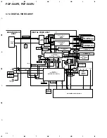
Page 31: ...VADR2 BRIDGE C ASSY BGC1 CLAMP ADR RESONANCE ASSY SUB ADDRESS B ASSY Q6706 Q6711 VADR Gen K2 K1 SAB3 SAB1 SAB2 VADR2 ADR_CO 60 IC5 VCC_VH PSUS VCP VC_VF VC_VF V_OFS VCC_VH V_IC5V V 3V_I V 3V V 3V_IC V 2V_IC V 2V_I V 5V_STB TXD RX I2 LED_SIG RE TXD0 RX0 V 3V V 3V BA2 9 PSUS Y SUS MASK Block PSUS IC6202 ADD SEL_PULSE IC5 VCC_VH IC6203 ADD SEL_PULSE IC5 VCC_VH IC6204 ADD SEL_PULSE IC5 VCC_VH IC6205 A...

Page 32: ...rd Release Driver IC Driver IC V 5V_ST V 5V_ST 12V Driver IC Driver IC Driver IC Driver IC ADR CONNECT B ASSY AB1 R21 R2 R26 R23 A24 A22 A21 R24 R11 R22 R3 CLK LE Driver IC Driver IC Driver IC Driver IC IC6501 Buffer IC Driver IC Driver IC Driver IC Driver IC Driver IC Driver IC ADR CONNECT A ASSY AA1 CLK LE VADR2 VADR2 BRIDGE D ASSY BGD1 CLAMP CLAMP D ASSY CLD1 VADR2 CLAMP K3 VADR2 5V 15V VCP 5V ...

Page 33: ...BUFF CCKM IC4007 COMPR SW_TRG F_KEY1 F_KEY2 Q4011 DRIVER LED_G LED_R I2C Q4401 BUFF L_CH Q4402 BUFF LED_G LED_R REM KEY1 KEY2 SPR SPL R_CH CN4401 CN4007 CN4009 C4043 HPF IC4010 NON_SYSTEM_DET R4093 R4098 BIAS IC4013 STB_DET S4001 S4004 etc MODEL_INFO IC4011 I O_EXPANDER Q4005 Q4006 5V 3 3V I2C_LEVEL_SHIFT IC4204 IC4203 CONF_ROM IC4201 DDC_ROM Q4201 Q4202 5V 3 3V I2C_LEVEL_SHIFT TMDS_RXCORE CONTENT...

Page 34: ...ave 0 3 3V swing square wave 0 3 3V swing square wave 0 3 3V swing square wave 0 3 3V swing square wave 0 3 3V swing square wave 0 3 3V swing square wave 0 3 3V swing square wave 0 3 3V swing square wave 0 3 3V swing square wave 0 3 3V swing square wave 0 3 3V swing square wave 0 3 3V swing square wave 0 3 3V swing square wave 0 3 3V swing square wave 0 3 3V swing square wave 0 3 3V swing square w...

Page 35: ...t section ADR CONNECT A D Assy Right section Y DRIVE Assy X DRIVE Assy ADR RESONANCE Assy 5V 5V PC_VIDEO ADR_K_EMG STOPB 3 3V 3 3V 12V ADR K PD U ADR PD APD MUTE EXD TXD RST2 RST PU EXD RXD RESET RESET RXD BUSY REQ_PU ADR K PD D DEW DET RELAY TEMP1 STB5V STB5V STB5V 3 3V 2 5V 3 3V 3 3V 3 3V VD HD VD 31 APLR STB5V 2 5V IIC BUS RGB 2 phase 8 bit VD HD DE CLK Address BUS Data BUS Control Signal TXDO ...

Page 36: ...0 Pulse Module IC3201 STK795 460 Pulse Module T3701 VRN D D CONV XCP MSK XSUS MSK VCP PLD SUSOUT A 37 40 29 30 K3105 PSUS K3107 IC3103 IC3104 TND301S Q3103 Q3107 Q3104 Q3109 Q3105 Q3124 Q3106 Q3125 SUSOUT B 37 40 29 30 K3106 IC3106 IC3107 TND301S Q3110 Q3114 Q3111 Q3115 Q3112 Q3126 Q3113 Q3127 To X CONNECTOR ASSY IC3110 TND301S IC3113 TND301S charge pump circuit From DIGITAL VIDEO ASSY Photo coupl...

Page 37: ...006 PE1013 IC2005 TC74ACT541FT Dew DET circuit Photo Coupler OC2 2 Y3 Y5 Photo Coupler SUS muteDET circuit charge pump circuit Photo Coupler VOFS D D CONV D GND 13 5V SUSGND D GND IC5V VF D D CONV IC5V UVP VOFS UVP VOFS OVP VH UVP VH OVP VOFS VF IC5V VF VH YSOFT D YOFS YCP MSK VH VH IC5V 13 5V 9V IC2208 HCPL M611 IC2001 TC74ACT541FT Q2102 IC2504 TC74ACT540FT IC2506 TC74ACT540FT IC2503 TC74ACT540FT...

Page 38: ...29 30 IC2201 TC74ACT541FT K2212 K2203 K2220 PSUS IC2212 TND301S Q2219 Q2218 IC2213 TND301S 2 9 11 18 Q2215 Q2216 Q2217 Q2226 IC2217 TND301S Q2227 Q2220 Q2221 Q2228 Q2232 Q2233 IC2216 TND301S YPR U1 YPR U2 VSUS SUSGND Q2210 Q2211 Q2212 Q2204 Q2205 IC2203 TND301S IC2204 TND301S IC2210 TND301S Vsus 15V 5V Vsus 15V 5V ...

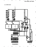
Page 39: ... D8804 DC AC AC 5V SW ADR D DC CLK ADR U ADR B 12V IC8802 IC8802 IC8803 DGND VADR ADRGND CLR ADROUT CN8803 IC8804 Current Voltage Convert Block Over Current DET Block ADR Output Resistance Load Block P D Output Block BUFF Block Inversion Block Additional Block Conparator EMG ON Flip Flop 5V REG H EMG1 OFF L EMG1 ON H V MID CLAMP OFF L V MID CLAMP ON Conparator EMG OFF 3 1 6 SUB ADDRESS A and B ASS...

Page 40: ...Q6708 ADR U Q6709 ADR D SW CN6701 ADR OUT L6704 IC6702 Q6702 Q6705 VADR V MID ADR D ADRGND C6722 Q6710 DGND Q6711 SW CN6703 DGND IC6703 Q6703 Q6712 V MID C6716 C6718 ADRGND ICP S1 0 ADR B Pre Drive ADR U Pre Drive ADR U Drive ADR D Pre Drive ADR D Drive ADR B Drive CAUTION FOR CONTINUED PROTECTION AGAINST RISK OF FIRE REPLACE ONLY WITH SAME TYPE NO ICP S1 0 MFD BY ROHM CO LTD FOR IC6704 3 1 7 ADR ...

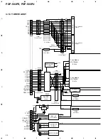
Page 41: ..._B DATA_R DATA_G DATA_B DATA_R DATA_G DATA_B DATA_R DATA_G DATA_B DATA_R DATA_G DATA_B DATA_R DATA_G DATA_B DATA_R DATA_G DATA_B HZ LBLK HBLK LE CLK V MID CLAMP U Output Block D9010 VADR U V MID U ADRGND U Q9006 NC DGND U NC SW U CN9002 R9012 Q9002 Q9004 R9014 V MID CLAMP L Output Block D9019 VADR L V MID L ADRGND L Q9005 DGND L SW L CN9001 R9011 Q9001 Q9003 R9013 V MID CLAMP Reference Voltage Blo...

Page 42: ... IC5201 NJM2193L IC5202 CXA2021S IC5002 LA4628 No Voltage V No Voltage V 1 5 9 12 5 25 2 0 13 1 73 3 5 95 14 5 95 4 5 94 15 5 92 5 5 98 16 5 91 6 6 02 17 5 93 7 6 02 18 5 92 8 7 38 19 5 94 9 5 95 20 5 95 10 1 55 21 11 91 11 5 24 22 5 9 No Voltage V No Voltage V 1 5 95 16 11 91 2 5 94 17 0 3 5 84 18 0 4 5 98 19 5 98 5 5 98 20 5 91 6 5 97 21 5 97 7 5 98 22 5 98 8 5 98 23 5 98 9 5 98 24 5 98 10 5 97 ...

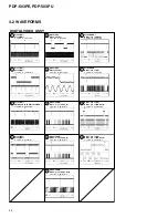
Page 43: ... 8 YSUS_B V 2V div H 2msec div 7 K1308 VDRB R1343 pin 8 RDAT_DL0 V 2V div H 4msec div 8 K1308 VDRB IC1501 pin 15 LBLK V 2V div H 2msec div 9 K1308 VDRB IC1501 pin 13 LE V 2V div H 2msec div 10 IC1501 pin 13 LE IC1501 pin 11 ADRCLK V 2V div H 200nsec div 10 IC1501 pin 13 LE IC1501 pin 11 ADRCLK V 2V div H 20nsec div 1 K1327 VDI K1328 HDI V 2V div H 10µsec div 2 K1327 VDI CN1004 pin 49 R DIGITAL VID...

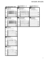
Page 44: ...c div Input VIDEO Signal Color bar 1 CH1 IC8801 pin 3 CH2 IC8801 pin 7 CH3 IC8802 pin 1 V 2V div H 2msec div Input VIDEO Signal Color bar CH1 H 2msec div CH2 CH3 V MID CLAMP ASSY 2 CH1 Q9006 Base CLAMP REF V CH2 D9010 Anode MID CH3 Q9006 Collector V 10V div H 2msec div Input PC Signal Color bar 1 CH1 Q9006 Base CLAMP REF V CH2 D9010 Anode MID CH3 Q9006 Collector V 10V div H 2msec div Input VIDEO S...

Page 45: ...iv 8 CN5301 pin 1 L GND V 1V div H 0 2msec div 7 1 10 9 CN5301 pin 2 L GND V 1V div H 0 2msec div 10 CN5301 pin 1 L pin 2 L V 2V div H 0 2msec div AUDIO SECTION Video Input Signal FULL FIELD COLOR BAR Audio Input Signal 1kHz Sine Carve 0 2Vrms Volume 60 MAX AV Selection STANDARD SRS OFF FOCUS OFF Measurement condition GND and the speaker output side becomes a short state on the oscilloscope Wrong ...

Page 46: ...µsec div Sustain Waveform sustain ch 1 K3107 X PSUS K3201 SUSGND V 50V div H 2µsec div ch 2 K2220 Y PSUS K2219 SUSGND V 50V div H 2µsec div Sustain Waveform reset pulse ch 1 K3107 X PSUS K3201 SUSGND V 100V div H 5µsec div ch 2 K2220 Y PSUS K2219 SUSGND V 100V div H 5µsec div Y Drive Pulse Control Waveform 1 field ch 1 K2220 Y PSUS K2219 SUSGND V 100V div H 2msec div ch 2 K2039 YCP_MSK K2024 DGND ...

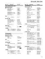
Page 47: ...0 C6007 C6008 C6014 C6019 C6025 CCSRCH181J50 C6028 C6035 C6039 C6046 C6047 CCSRCH181J50 C6056 C6057 CCSRCH181J50 C6003 C6006 C6017 C6018 C6020 CCSRCH390J50 C6023 C6024 C6029 C6033 C6034 CCSRCH390J50 C6037 C6043 C6045 C6049 C6053 CCSRCH390J50 C6055 C6060 C6062 C6066 CCSRCH390J50 C6010 C6016 C6030 C6036 C6050 CKSRYF104Z16 C6061 CKSRYF104Z16 RESISTORS R6007 R6012 R6021 R6028 R6032 RAB4C221J R6040 RAB...

Page 48: ...istors RS1 16S J X CONNECTOR B ASSY RESISTORS All Resistors RS1 16S J BRIDGE A ASSY SEMICONDUCTORS D6421 D6422 D1FL20U S CAPACITORS C6421 C6422 0 1µF 100V ACG1098 OTHERS CN6421 PH CONNECTOR B4B PH SM3 BRIDGE B ASSY SEMICONDUCTORS D6431 D6432 D1FL20U S CAPACITORS C6431 C6432 0 1µF 100V ACG1098 OTHERS CN6431 PH CONNECTOR B4B PH SM3 BRIDGE C ASSY SEMICONDUCTORS D6441 D6442 D1FL20U S CAPACITORS C6441 ...

Page 49: ...Z16 RESISTORS R6618 R6622 R6624 R6626 R6628 RAB4C100J R6630 R6631 R6633 R6637 R6639 RAB4C100J R6641 R6643 R6645 R6647 RAB4C100J R6616 RAB4C473J Other Resistors RS1 16S J OTHERS CN6601 55P CONNECTOR AKM1202 ADR CONNECT C ASSY SEMICONDUCTORS IC6801 TC74VHC541FT Q6802 2SC2712 Q6803 2SK209 D6801 DA227 COILS L6801 L6802 22µH 0 11A ATH1081 CAPACITORS C6811 C6820 330pF 100V ACG1094 C6831 C6833 C6834 47µF...

Page 50: ...00 IC3201 STK795 460 IC3101 TC74ACT541FT IC3103 IC3104 IC3106 IC3107 TND301S IC3110 IC3113 TND301S IC3109 UPC78L05T Q3117 2SJ181L Q3116 Q3119 Q3120 2SJ522 Q3101 2SK2503 Q3103 Q3107 Q3109 Q3115 FS16VS 9 Q3124 Q3127 FS16VS 9 Q3123 FS2AS 14A Q3122 Q3128 FS7VS 14A Q3102 Q3118 HN1B04FU D3119 1SS184 D3108 D3124 D3125 D3130 D3133 1SS355 D3101 D3102 D3117 D3126 D3131 D1FL40 D3200 D3202 D3203 D3205 D1FL40 ...

Page 51: ...823J VR3701 1kΩ ACP1089 Other Resistors RS1 16S J Y DRIVE ASSY Y DRIVE LOGIC BLOCK SEMICONDUCTORS IC2006 PE1013B IC2007 TC74ACT540FT IC2001 IC2003 IC2005 TC74ACT541FT Q2121 2SK2201 Q2101 Q2102 HN1C01FU D2101 1SS355 COIL L2001 LFEA100J CAPACITORS C2101 CEHAT100M50 C2103 CEHAT1R0M50 C2003 CEHAT470M16 C2001 C2004 C2005 C2007 C2008 CKSRYF104Z50 C2010 C2102 C2104 C2121 CKSRYF104Z50 RESISTORS R2015 R201...

Page 52: ...2MMF4R7J R2277 RS3LMFR47J R2276 RS3LMFR56J VR2201 VR2204 1kΩ ACP1089 Other Resistors RS1 16S J OTHERS SPACER AEH1049 K2211 K2214 K2217 TEST PIN AKX9002 KN2201 KN2210 GROUND PLATE ANK 142 CN2201 15P PLUG KM250MA15 CN2202 3P PLUG KM250MA3 Y DRIVE SCAN BLOCK SEMICONDUCTORS IC2501 IC2502 IC2505 IC2510 HCPL M611 IC2512 IC2514 IC2516 IC2525 HCPL M611 IC2503 IC2504 IC2506 TC74ACT540FT COILS L2501 L2503 L...

Page 53: ...Q8806 2SK209 D8801 D8803 D8809 1SS355 D8806 D8807 DA227 D8808 UDZ27B D8804 UDZS5 1B COILS L8801 CHOKE COIL 100µH 0 45A ATH1074 L8802 L8803 COIL 22µH 0 11A ATH1081 CAPACITORS C8806 CCSRCH101J50 C8822 CEHV100M16 C8804 CEHV100M35 C8801 C8808 CEHV470M16 C8807 CEVNP2R2M35 C8802 C8803 C8805 C8809 C8817 CKSRYF104Z16 C8820 C8821 CKSRYF104Z16 RESISTORS R8806 R8807 R8837 R8838 R8841 RS1 16S1002D R8858 RS1 1...

Page 54: ...S K1101 K1104 K1107 K1108 AKX9002 TEST PIN X1101 CERAMIC RESONATOR ASS1160 25MHz MODULE UCOM BLOCK SEMICONDUCTORS IC1204 24LC04B I SN IC1208 PST9246N IC1202 TC74VHC08FT IC1201 TC74VHC21FT IC1205 TC74VHC541FT IC1203 TC74VHCT541AFT IC1206 TC7W126FU D1201 D1202 1SS355 CAPACITORS C1213 C1243 C1245 CCSRCH470J50 C1235 C1236 CCSRCH7R0D50 C1225 C1232 CEV470M6R3 C1201 C1203 C1206 C1211 CKSRYB102K50 C1214 C...

Page 55: ...0J Other Resistors RS1 16S J OTHERS K1901 K1906 TEST PIN AKX9002 1901 DC DC CONVERTER AXY1054 CN1901 PH CONNECTOR B13B PH SM3 MR INTERFACE ASSY INTERFACE BLOCK SEMICONDUCTORS IC4011 CXA1875AM IC4007 IC4010 M5223AFP IC4005 M62320FP IC4001 PQ05DZ51 IC4002 IC4004 PQ20VZ1U IC4013 PST9228N IC4008 IC4009 TC74HC00AF IC4012 TC74HC4066AF IC4006 TC74VHCT541AFT Q4003 Q4004 Q4010 2SA1162 Q4007 Q4009 Q4013 Q40...

Page 56: ... C4213 C4216 C4218 C4221 C4225 CKSRYF104Z16 C4234 C4235 C4240 C4243 C4245 CKSRYF104Z16 C4247 C4251 C4252 C4256 C4259 CKSRYF104Z16 C4261 CKSRYF104Z16 C4223 C4226 C4228 C4249 CKSRYF105Z10 C4266 C4270 CKSRYF105Z10 RESISTORS R4213 R4217 R4245 R4247 RAB4C181J R4253 R4255 RAB4C181J R4241 RAB4C680J R4250 RS1 16S5100D Other Resistors RS1 16S J OTHERS K4201 K4207 TEST PIN AKX9002 X4201 CRYSTAL RESONATOR AS...

Page 57: ...J50 C5237 CFTLA103J50 C5035 C5046 C5053 C5056 C5216 CFTLA104J50 C5221 C5239 CFTLA104J50 C5214 C5230 CFTLA224J50 C5225 CFTLA333J50 C5219 C5236 CFTLA473J50 C5003 C5006 C5016 C5042 C5207 CKCYB103K50 C5210 CKCYB103K50 C5043 C5052 C5205 C5229 CQMA122J50 C5224 CQMA222J50 C5215 C5231 CQMA392J50 RESISTORS R5053 R5054 R5075 R5076 RD1 2MMF2R2J R5001 RD1 2MMF3R9J Other Resistors RD1 4PU J OTHERS J5003 6P HOU...

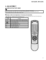
Page 58: ...DP R03E or PDP R03U Perform the adjustment and setting in the state that this unit and Media Receiver are connected by the system Plasma display cannot use a factory mode by being simple Remote Control Key Function P key One line moves the selection cursor of the adjustment item up P key One line moves the selection cursor of the adjustment item down VOL key 1 raises a adjustment value VOL key 1 r...

Page 59: ...andby state Confirm that the plasma display and the media receiver turned on together and a system cable is connected properly Image receiving state Page 1 13 General information of the Plasma Display and Media Receiver Service Factory Mode Page 2 13 to 9 13 Adjustment and setting item of the Media Receiver Page 11 13 to 13 13 Adjustment and setting item of the Plasma Display Note 1 When use the a...

Page 60: ...mputer version information of the PDP 7 Panel flash ROM version information of the PDP 8 PDP model information 01 PIONEER 50 inches 02 PIONEER 43 inches 11 SHARP 50 inches 12 SHARP 43 inches 9 Media receiver model information 10 Media receiver model information 11 PDP destination information 0 All SHARP destinations Japanese and North America destinations of PIONEER 3 European and general destinat...

Page 61: ...value PDP 9 BLUE_OFS of PDP_W B table 1 0 to 999 Factory adjustment value PDP 10 RED_GAIN of PDP_W B table 2 0 to 255 Factory adjustment value PDP 11 GREEN_GAIN of PDP_W B table 2 0 to 255 Factory adjustment value PDP 12 BLUE_GAIN of PDP_W B table 2 0 to 255 Factory adjustment value PDP 13 RED_OFS of PDP_W B table 2 0 to 999 Factory adjustment value PDP 14 GREEN_OFS of PDP_W B table 2 0 to 999 Fac...

Page 62: ...alue PDP 7 SUS_B timing setting of Y drive 0 to 15 Factory adjustment value PDP 8 SUS_G timing setting of Y drive 0 to 15 Factory adjustment value PDP Adjustment item of this page is related in damage of the set when mistakes adjustment When adjustment is needed be enough careful to adjustment Caution in the electric power setting No 1 and 2 adjustment Adjustment value is reflected without relatio...

Page 63: ...nal screen in the PDP inside signal generation A pattern mask and a full mask can use only either Therefore turn a full mask to OFF when uses a pattern mask Also turn a pattern mask to OFF when uses a full mask A pattern mask and a full mask are test signal screens occurring together in the PDP inside Therefore in the mask signal generation it cannot confirm video inputting from OSD and the outsid...

Page 64: ...oard to replace and install it to the new PC Board Y DRIVE Assy When repaired When replaced 1 VOFS VH IC5V voltage adjustment 2 Timing adjustment of pulse module 1 SUSB ground timing adjustment 2 Panel white balance adjustment 1 SUSB ground timing adjustment 2 Panel white balance adjustment X DRIVE Assy When repaired When replaced 1 VRN voltage adjustment 2 Timing adjustment of pulse module DIGITA...

Page 65: ...ircuit PSUS GNDH and another GND because that may damage the unit The symptom is case of mis adjustment If the VOFS Voltage adjustment is not performed properly dots like blinking luminance points appear If deviated greatly from the right adjustment point panel will light white VR2702 IC5V Y DRIVE Assy Note Be sure to measure between specified test points Input Command DAC Output Setting Voltage I...

Page 66: ... becomes 300V 1 0V Input Signal Adjusting Point Adjusting Method Reference Adjustment values using the Media color difference meter A 100 Adjust the parameter in the OFFSET DIGITAL of factory mode as follows PANEL R HIGH PANEL B LOW In this time dispay uses the mask MASK04 of factory mode Sustain Pulse Waveform Adjustment VRN Voltage Adjustment Panel White Balance Adjustment MASK Left Side x 295 y...

Page 67: ...istance value of SUS B and SUS G to match VR resistance value of SUS D within 2Ω Power OFF Adjustment end SUS D readjustment Adjust the waveform to 20 25ns SUS U readjustment Adjust the waveform to 20 25ns X DRIVE Y DRIVE SUS U VR3203 VR2204 SUS D VR3202 VR2203 SUS B VR3201 VR2202 SUS G VR3200 VR2201 Pulse Module X DRIVE Y DRIVE Upper Lower Upper Lower SUSOUT K3105 K3106 K2212 K2203 SUS U K3200 K3...

Page 68: ...ms div 5µs div 1SF 2SF 3SF 4SF 5SF 6SF 7SF 1ms div 5µs div Perform adjustment of waveform with a black mask screen It is easy to adjust when turned field AB offset to OFF RS 232C command OCN in adjustment Note Sampling rate of oscilloscope sets it more than 500MS s in order to perform ns order adjustment Collecting calibration of probe before adjustment by all means Connect GND of probe measuring ...

Page 69: ...orm of CH1 CH2 of the part which enclosed in the following circle whether there is not a large gap A gap of the quantity that shifts 20nS and adjusted remains When adjust in the power supply ON state change so that the quantity of gap that adjusted by temperature rise of the pulse module becomes small Therefore perform high power OFF RS 232C command DRF except measurement time of waveform when adj...

Page 70: ...n SUS B becomes ON Adjust so that the voltage of this inflection point is the nearest to 150V and do not become less than 150V Adjustment parameter X DRIVE XSUSB RS 232C command XSB Y DRIVE YSUSB RS 232C command YSB Note Connect GND of probe measuring waveform to SUSGND terminal by all means Precise waveform is not displayed and an adjustment gap may occur that does not collect GND properly Wavefo...

Page 71: ... OFS K2039 YSUS_MSK K2037 YSUS_G K2028 YSUS_U K2021 YPR_U2 K2029 YSUS_D K2027 YSUS_B K2024 DGND K2101 DEW_DET K2043 DGND K2008 DGND K2007 DGND K2006 5V K2707 IC5V K2714 GNDHS K2704 VF K2701 VF K2706 14V K2711 8V K2713 IC5V UVP VR3200 SUS G VR3201 SUS B VR3202 SUS D VR3203 SUS U K3103 VCP_PD K3104 5V K3001 5V K3003 XSUS B K3015 XSUS MSK K3017 XCP MSK K3012 XSUS D K3014 XNR D1 K3025 K3007 K3010 XNR ...

Page 72: ... bps is fixed Communication baudrate PDP rear view DVI Video line Input optional video from the signal source with the DVI output Input timing is as follows Communication line Connect a system cable PC for control Connect to DSUB 9 pin DSUB 9 pin straight cable Exclusive use communication jig AC DC adapter 9V or 12V output DVI input timing XGA60 VESA conformity CLK 65MHz H total 1344 clk H disp 10...

Page 73: ...13 12 11 10 9 C1 V C1 C2 C2 V DOUT2 RIN2 VCC GND DOUT1 RIN1 ROUT1 DIN1 DIN2 ROUT2 C3 1 50 C5 47 16 C7 47 16 C8 0 1 C4 0 1 C2 1 50 C6 R14 100k 1 50 L G_JIGU10 R15 100k R12 2 2k R11 2 2k R16 10k R17 10k R1 1k R3 0 R2 0 C9 0 1 G_JIGU10 C10 47 16 VIN VO VC GND NC R6 100 R13 0 R7 100 V_JIGU10 R9 0 R10 SP_L CSEN1 CSEN2 CCKM GND SMPOW SP_R SENCE GND RXD0_M SP_L GND SRST FLASH_W GND SR_UP SR_DOWN SP_R GND...

Page 74: ...d a B W e h t e r i u q c A 1 S G 1 S U T A T S T E G n o i t a m r o f n i n o i s r e v e h t e r i u q c A S M H T E S R E T E M R U O H e m i t l a n o i t p o o t r e t e m r u o h t e S 0 0 M 0 0 K S A M F F O e d o m k s a M 1 0 M 1 0 K S A M p m a L 1 n r e t t a P 2 0 M 2 0 K S A M r a b r o l o C 2 n r e t t a P 3 0 M 3 0 K S A M e n i l g n i t n a l S 3 n r e t t a P 4 0 M 4 0 K S A M ...

Page 75: ... o t l e n a p e h t f o t h g i l h g i h B W e h t t e S N L P O N E C N A H N E T H G I R B F F O e c n a h n e n o i t c e r r o c s s e n t h g i r b r e t n e C Y L P S E Y E C N A H N E T H G I R B N O e c n a h n e n o i t c e r r o c s s e n t h g i r b r e t n e C S M P T E S R E T E M E S L U P r e t e m e s l u p e h t f o g n i t t e s l a n o i t p O F O P F F O R E W O P t s e u q e...

Page 76: ...f W B adjustment value Green Reference data 3 byte 5 Offset data 3 byte Note 1 6 Gain of W B adjustment value Blue Reference data 3 byte 7 Offset data 3 byte Note 1 8 Offset of W B adjustment value Red Reference data 3 byte 9 Offset data 3 byte Note 1 10 Offset of W B adjustment value Green Reference data 3 byte 11 Offset data 3 byte Note 1 12 Offset of W B adjustment value Blue Reference data 3 b...

Page 77: ...on 3 byte 4 Panel microcomputer version 3 byte 5 Panel FLASH ROM version 3 byte 6 Hour meter hour 5 byte Unit H time 7 Pulse meter 7 byte Unit 0 01G 10 000 000 8 Main microcomputer model number 4 byte 5692 or F692 9 Main microcomputer version 3 byte 10 Wide microcomputer version 3 byte 11 Wide FLASH ROM version 3 byte Data Model MX5 PDP 503MX initial value MX4 PDP 433MX MD5 Module 50 inches MD4 Mo...

Page 78: ... CONNECTOR B Assy FRONT KEY Assy LED Assy SP TERMINAL Assy X DRIVE Assy AUDIO AMP Assy ADR CONNECT A Assy Y DRIVE Assy SCAN A Assy THERMAL SENSOR Assy BRIDGE A Assy SCAN B Assy ADR CONNECT B Assy ADR RESONANCE Assy SUB ADDRESS A Assy SUB ADDRESS B Assy ADR RESONANCE Assy ADR CONNECT C Assy ADR CONNECT D Assy CLAMP A Assy ADR CONNECT C Assy MR INTERFACE Assy SW POWER SUPPLY Module BRIDGE C Assy BRI...

Page 79: ...simultaneously display LED in order to 1st 2nd Examples LED blinks in the 1st power down Y DC DC CONVERTER 2nd power down Y DRIVE Number of blinks Name 1 Panel Microcomputer NG 2 DIGITAL IIC communication NG 3 Dewdrop abnormality 4 Temperature abnormality Number of blinks Name 1 Y DRIVE 2 Y DC DC CONVERTER 3 X DC DC CONVERTER 4 X DRIVE 5 Power supply 6 Address junction 7 Address resonance 8 DIGITA...

Page 80: ...P1 DIGITAL VIDEO ASSY THERMAL SENSOR ASSY Y DRIVE ASSY SW POWER SUPPLY MODULE MR INTERFACE ASSY AUDIO ASSY MEDIA RECEIVER IC1191 Panel UCOM external Flash ROM IC1204 EEPROM IC1101 Panel UCOM IC1207 Module UCOM IC4204 SiI861 IC5202 CXA2021S IC4005 Expander IC4011 Expander Expander SCL SDA A_SCL A_SDA DDC_SCL DDC_SDA D1 D3 P2 R3 D18 TE1 D6 Y2 1 4 3 2 2 2 IC8351 Thermal Sensor 1 Moisture Sensor ...

Page 81: ...Disconnect a connector CN2002 between Dew drop sensor and Y DRIVE Assy 3 Dew drop detection When temperature of this unit became abnormally high this NG occurs Shut down after OSD display from the NG detection for 30 seconds Note When temperature fell down during indication return to the normal operation Abnormality to expect when it occurs in the environment that is not high temperature Disconnec...

Page 82: ... OR OR OR D8 D11 8 6 7 4 5 1 2 3 ADR CONNECT ASSY Upper DIGITAL VIDEO ASSY SW POWER SUPPLY MODULE X DRIVE ASSY Y DRIVE ASSY ADR CONNECT ASSY Lower RESONANCE ASSY Upper RESONANCE ASSY Lower D12 D16 D1 X1 P4 P2 P3 Y1 D17 D15 IC1201 pin 8 IC1201 pin 6 D1202 Cathode DIG_ADR PD PD_TRIGGER Note 1 8 show LED flashing number of times when power down occurred in this route ...

Page 83: ...y VSUS overvoltage VSUS UVP P D by VSUS undervoltage overcurrent VADR OVP P D by VADR overvoltage VADR UVP P D by VADR undervoltage overcurrent 15V OVP P D by 15V overvoltage 15V UVP P D by 15V undervoltage overcurrent 12V UVP P D by 12V undervoltage overcurrent 6 5V OVP P D by 6 5V overvoltage 6 5V UVP P D by 6 5V undervoltage overcurrent 13 5V UVP P D by 13 5V undervoltage overcurrent 9V UVP P D...

Page 84: ...E X DRIVE Assy IC3200 IC3201 pulse module IC3103 IC3104 IC3106 IC3107 IC3110 IC3113 R3109 K3103 Lo VCP OCP Q3122 K3102 Lo VRN OCP 5 PS X DRIVE Assy IC3200 IC3201 Pulse module When P4 connector disconnected P D does not occur Y DRIVE Assy IC2206 IC2214 Pulse module When P3 connector disconnected P D does not occur MX AUDIO Assy IC8601 Audio IC When P6 connector disconnected P D does not occur When ...

Page 85: ... VOFS voltage and not for the VSUS voltage and it is controlled by software 4 When a fuse blows If a fuse blows never turn the power on again only after replacing the fuse In most cases the fuse itself did not have any problem So as long as factors of overcurrent have not been removed chances of destruction increase every time the power is turned on In the worst case about a dozen parts may be des...

Page 86: ...er when a rear case of plasma display was opened carelessly Detect switch does not detect at the power supply OFF and the remote control unit wait state Please stick this detect switch with tape before turning on the power in inside diagnoses of the plasma display And please remove it not to forget the tape which stuck after the repair When detect switch has worked by any chance When detect switch...

Page 87: ...he DIGITAL VIDEO Assy Connector Circuit Board Spacer 6 2 Remove the SW Power Supply Module Connector Screws 4 MR INTERFACE AUDIO AMP SP TERMINAL and DIGITAL VIDEO Assys MR INTERFACE Assy SP TERMINAL Assy IF Earth Metal AUDIO AMP Assy DIGITAL VIDEO Assy 6 6 6 5 Insert it and reduce the Clamper Clamper Sub Frame L Slit SW Power Supply Module Sub Frame R 6 Insert the SW Power Supply Module into the s...

Page 88: ... top of Front Case 50 P 6 6 Remove the Front Case 50 P 3 10 10 7 Remove the Rear Case 50P Screws 19 8 Remove the Y DRIVE Assy Connector Screws 8 9 Remove the Front Chassis V Screws 5 10 Reverse the SCAN A and SCAN B Assemblies 11 When it is necessary exchange the ROM Y DRIVE SCAN A B Assy 1 Front Case 50 P Front Case 50 P Aluminum Materials It is the structure that a hook of Front Case 50 P was pu...

Page 89: ...88 PDP 503PE PDP 503PU 1 Remove the Rear Case 50P Screws 19 2 Remove the X DRIVE Assy Connector Screws 8 X DRIVE Assy 2 2 2 2 2 2 2 2 X DRIVE Assy ...

Page 90: ...IC6006 Scan IC 1 10 20 30 40 90 50 60 70 HVO35 HVO36 HVO37 HVO38 HVO39 HVO40 HVO41 HVO42 HVO43 HVO44 HVO45 HVO46 HVO47 HVO48 HVO49 HVO50 HVO51 HVO52 HVO53 HVO54 HVO55 HVO56 HVO57 HVO58 HVO59 HVO60 HVO61 HVO62 HVO63 HVO64 HVO30 HVO29 HVO28 HVO27 HVO26 HVO25 HVO24 HVO23 HVO22 HVO21 HVO20 HVO19 HVO18 HVO17 HVO16 HVO15 HVO14 HVO13 HVO12 HVO11 HVO10 HVO34 HVO33 NC VH2 VH2 NC GND GND GND GND NC GND GND ...

Page 91: ...tional control signal of shift register CLR 45 I 1 It do data of shift register with L by L level OC1 42 I 1 An output control terminal of HVO OC2 43 I 1 An output control terminal of HVO HVO 1 30 51 82 99 100 O 64 High voltage drive output HVO1 HVO64 VDD 41 1 Logic power supply GND 34 35 38 46 47 87 89 91 94 12 Standard potential This is common to HVO1 HVO64 VH1 84 85 49 50 4 The high potential c...

Page 92: ...A15 Address bus 24 UA16 Address bus 25 UA17 Address bus 26 UA18 Address bus 27 UA19 Address bus 28 VSS GND 29 UA20 Address bus 30 PA5 NC terminal 31 PA6 NC terminal 32 PA7 NC terminal 33 CE_PN Enables for panel microcomputer 34 CE_PN Enables for panel microcomputer 35 VSS GND 36 VSS GND 37 APLP The APL value acquisition trigger signal input 38 VD_31 The V signal input from IC1401 PD6358 39 VCC 3 3...

Page 93: ...essage lye Norwich output 74 REQ_PU A communication demand to a module microcomputer 75 SEL23B IC1703 PE5064 control terminal 76 CLRB IC1703 PE5064 control terminal 77 FR_SEL The free run select signal output 78 RST31B The reset output to IC1301 IC1401 PD6358 79 RST23B The reset output to IC1703 PE5064 80 FWE Microcomputer program note control signal 81 RESET Reset input 82 NMI The at the rate of ...

Page 94: ...e emergency input from panel upper address resonance block unused 112 P47 NC terminal 113 AVSS GND 114 VSS GND 115 MUTE_ADR The panel mute signal input 116 MUTE_SUS The X and Y drive mute signal output unused 117 P15 NC terminal 118 HD The HD signal input from outside Assy RGB Assy etc 119 P13 NC terminal 120 P12 NC terminal 121 PC_VIDEO The PC Video identification output 122 VD The HD signal inpu...

Page 95: ...4 1_23 1_39 22 XSUS_DI 4 XSUS_DO 1_48 1_5 1_22 1_40 21 XSUS_GI 6 YSUS_GO 1_45 1_1 1_55 1_54 19 XNR_D1I 7 XNR_D1O 1_44 1_51 1_62 1_36 18 XNR_D2I 10 XNR_D2O 1_43 1_2 1_61 1_35 15 XSUS_MSKI 8 XSUS_MSKO 1_46 1_32 1_28 1_41 17 XCP_MSKI 9 XCP_MSKO 1_47 1_31 1_34 1_42 16 XNR_UI 5 XNR_UO 1_57 1_58 1_60 1_56 20 1_52 1_53 PE1013B X DRIVE ASSY IC3003 Drive Protect PLD Pin Assignment Top View Block Diagram ...

Page 96: ...ypru1in 6 1_3 1_13 ypru2in 1_2 1_16 yofsin 1_1 1_15 ysofdin 1_10 1_52 ysusmskin 1_9 1_12 ycpmskin 10 1_8 1_11 1_26 1_53 1_62 1_61 1_27 1_28 1_60 1_59 1_66 1_56 1_54 1_33 1_55 1_37 1_49 1_51 1_41 16 ysoftdout 1_42 14 yofsout 1_43 20 ypru2out 1_44 18 ypru1out 1_45 19 ysusgout 1_46 17 ysusdout 1_47 21 ysusuout 1_48 22 ysusbout 1_39 23 ycpmskout 1_40 15 7 5 11 9 4 PE1013B Y DRIVE ASSY IC2006 Drive Pro...

Page 97: ... N 8 2 C N l a n i m r e t C N 9 2 L C S Y S S A y l p p u s r e w o p h t i w n o i t a c i n u m m o c C I I M O R P E E 0 3 A D S Y S S A y l p p u s r e w o p h t i w n o i t a c i n u m m o c C I I M O R P E E 1 3 1 D X T e t o n m a r g o r p a e d i s t u o e h t h t i w n o i t a c i n u m m o C 2 3 1 D X R e t o n m a r g o r p a e d i s t u o e h t h t i w n o i t a c i n u m m o C 3 3 1...

Page 98: ... o c o r c i m l e n a P 6 7 C N l a n i m r e t C N 7 7 L C S _ C D D r e v i e c e r a i d e m a h t i w n o i t a c i n u m m o c C I I 8 7 A D S _ C D D r e v i e c e r a i d e m a h t i w n o i t a c i n u m m o c C I I 9 7 C N l a n i m r e t C N 0 8 C N l a n i m r e t C N 1 8 T E D _ W E D t u p n i r o s n e s n o i t a s n e d n o c w e d e h T 2 8 C N l a n i m r e t C N 3 8 C N l a n i...

Page 99: ... d d A 5 2 7 1 O R A l a n g i s R t u p t u o a t a d s s e r d d A 6 2 S S V D N G 7 2 7 1 O B A l a n g i s B t u p t u o a t a d s s e r d d A 8 2 7 1 O G A l a n g i s G t u p t u o a t a d s s e r d d A 9 2 8 1 O G A l a n g i s G t u p t u o a t a d s s e r d d A 0 3 9 1 O B A l a n g i s B t u p t u o a t a d s s e r d d A 1 3 5 1 T A D U s u b a t a d r e t u p m o c o r c i M 2 3 2 1 T A...

Page 100: ...u p n i l a n g i s t c e p s a B e r u t c i p R e h T 8 7 6 I B R t i b h t x i s e h t t u p n i l a n g i s t c e p s a B e r u t c i p R e h T 9 7 4 I B R t i b h t r u o f e h t t u p n i l a n g i s t c e p s a B e r u t c i p R e h T 0 8 9 0 S S V O D N G 1 8 B T S R t u p n i t e s e R 2 8 8 I B G t i b h t h g i e e h t t u p n i l a n g i s t c e p s a B e r u t c i p G e h T 3 8 8 1 E ...

Page 101: ...1 O B A l a n g i s B t u p t u o a t a d s s e r d d A 5 2 1 6 1 O G A l a n g i s G t u p t u o a t a d s s e r d d A 6 2 1 8 1 O R A l a n g i s R t u p t u o a t a d s s e r d d A 7 2 1 9 1 O G A l a n g i s G t u p t u o a t a d s s e r d d A 8 2 1 5 0 E D D V O y l p p u s r e w o p V 3 3 9 2 1 3 1 T A D U s u b a t a d r e t u p m o c o r c i M 0 3 1 0 1 T A D U s u b a t a d r e t u p m o ...

Page 102: ... 0 1 S S V O D N G 7 7 1 4 I B G t i b h t r u o f e h t t u p n i l a n g i s t c e p s a B e r u t c i p G e h T 8 7 1 1 I B G t i b t s r i f e h t t u p n i l a n g i s t c e p s a B e r u t c i p G e h T 9 7 1 9 I B B t i b h t n i n e h t t u p n i l a n g i s t c e p s a B e r u t c i p B e h T 0 8 1 5 I B B t i b h t f i f e h t t u p n i l a n g i s t c e p s a B e r u t c i p B e h T 1 8...

Page 103: ...u p m o c o r c i M 5 2 2 4 1 I R D A U s u b s s e r d d a r e t u p m o c o r c i M 6 2 2 9 0 E D D V O y l p p u s r e w o p V 3 3 7 2 2 1 1 I R D A U s u b s s e r d d a r e t u p m o c o r c i M 8 2 2 8 I R D A U s u b s s e r d d a r e t u p m o c o r c i M 9 2 2 4 I R D A U s u b s s e r d d a r e t u p m o c o r c i M 0 3 2 3 T I B t i b d r i h t e h t t u p t u o o N d l e i f b u S 1 3 ...

Page 104: ... r u t c i p R e h T 1 7 2 N U R E E R F t u p n i l o r t n o c n u r e e r f e h T 2 7 2 8 I A G t i b h t h g i e e h t t u p n i l a n g i s t c e p s a A e r u t c i p G e h T 3 7 2 5 I A G t i b h t f i f e h t t u p n i l a n g i s t c e p s a A e r u t c i p G e h T 4 7 2 1 I A G t i b t s r i f e h t t u p n i l a n g i s t c e p s a A e r u t c i p G e h T 5 7 2 8 I A B t i b h t h g i e...

Page 105: ... r d d A 6 2 3 C N l a n i m r e t C N 7 2 3 5 2 O G A l a n g i s G t u p t u o a t a d s s e r d d A 8 2 3 S S V D N G 9 2 3 3 2 O B A l a n g i s B t u p t u o a t a d s s e r d d A 0 3 3 E D D V y l p p u s r e w o p V 3 3 1 3 3 1 2 O B A l a n g i s B t u p t u o a t a d s s e r d d A 2 3 3 S S V D N G 3 3 3 D P V D N G 4 3 3 E D D V y l p p u s r e w o p V 3 3 5 3 3 0 I B R t i b 0 e h t t u...

Page 106: ...SOT 25 TOP VIEW Pin No Pin name Functions 1 TC SUB TPLH control pin Substate pin 2 3 GND GND pin 4 VOUT Reset signal output pin 5 VCC VCC pin voltage detect pin Pin Assignment Top View PST9246N DIGITAL VIDEO ASSY IC1208 Reset IC Block Diagram Pin Function ...

Page 107: ... to external clock other than crystal leave Xout pin2 unconnected 7 3 S0 S1 I CMOS TTL Digital control inputs to select input frequency range and output frequency scaling Refer to Tables 7 and 8 for selection S0 has internal pulldown S1 has internal pullup 4 LF I Analog Loop Filter Single ended tri state output of the phase detector A two pole passive loop filter is connected to Loop Filter LF 6 F...

Page 108: ...VCC VS VB HO 13 N C 17 N C 14 IN2 15 SD1 16 IN1 18 IN4 19 SD2 20 IN3 21 PL2 30 PL1 PL1 25 PC2 24 PC2 26 PC1 PC1 22 PL2 23 N C 31 N C 36 N C 34 POWER GND 35 POWER GND 33 POWER GND 32 POWER GND 28 N C 12 SUB GND 9 SIG GND 6 VCC 7 VDD 10 SIG GND TR1 TR8 R4 R9 R10 R3 TR3 TR4 VDD IC2 C5 C4 C6 TR9 TR5 TR6 D4 D3 R15 R5 D7 D5 D6 D8 D9 D10 HIN SD LIN VSS LO COM VCC VS VB HO TR10 R12 R11 R6 ZD1 R13 C7 C8 27...

Page 109: ...503PE PDP 503PU STANDBY ON INPUT STANDBY ON VOLUME CHANNEL MAIN POWER button Power indicator STANDBY ON button INPUT button VOLUME buttons CHANNEL buttons Remote control sensor Plasma Display 8 PANEL FACILITIES ...

Reviews: