background image

53

HTP-071

5

6

7

8

5

6

7

8

A

B

C

D

E

F

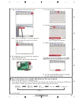
Select "CECCore_ADDSEL(BB)_V***.hex" file to update MCU.

When the update file is selecting, the check box is 
automatically on.

Rate of the progression is appeared.

17.  Select the update file. Press the "FILE" button.

19.  Press the     button.

20.  Press the    button to update the firmware.

21.  Update Finished CEC microcomputer.

22.  Turn the unit off (STA

N

DBY mode) and unplug the 


AC cord.  Disconnect the FFC cable.

18.  While holding down the tact switch of the Upgrade Jig, 
 press 

STA

N

DBY/O

N

 button.


After 2 or 3seconds, release the tact switch button.

24.  Turn the unit off.

23.  Make sure that the main unit is in STA

N

DBY mode.


Press and hold the " E

N

TER " and " STA

N

DBY/O

N

 " keys, then press the " E

N

TER "key to display each UCOM version. 


 Each time the " E

N

TER "key is pressed, then indications on the FL display change as follows:

If the following messages are displayed, shut the update 
program down, and start the update again from step 19.

Check to the software virsion of MAIN, HDMI (SUB) and  CEC microcomputers

"E

N

TER"

"E

N

TER"

"E

N

TER"

"E

N

TER"

"E

N

TER"

MAI

N

 Ucom

MAI

N

 Xx.xx

SUB Ucom
SUB zzz.zz

CEC
CEC Vy,yy

DSP Ucom

All segments lit.

Summary of Contents for HTP-071

Page 1: ... Front HTP 071 RRV4273 HOME CINEMA PACKAGE HTP 071 AUDIO VIDEO MULTI CHANNEL RECEIVER VSX 321 K P SUBWOOFER SPEAKER SYSTEM S 22W P S 11 P HTP 071 is a Home Cinema Package and consists of VSX 321 K P S 22W P and S 11 P THIS MANUAL IS APPLICABLE TO THE FOLLOWING MODEL S AND TYPE S Model HTP 071 SYXE8 AC 220 V to 230 V HTP 071 CXE AC 120 V HTP 071 DLPWXE AC 220 V to 240 V HTP 071 AXE5 AC 220 V VSX 32...

Page 2: ...60 Hz outlet and turn the AC power switch on Any current measured must not exceed 0 5 mA ANY MEASUREMENTS NOT WITHIN THE LIMITS OUTLINED ABOVE ARE INDICATIVE OF A POTENTIAL SHOCK HAZARD AND MUST BE CORRECTED BEFORE RETURNING THE APPLIANCE TO THE CUSTOMER 2 PRODUCT SAFETY NOTICE Many electrical and mechanical parts in the appliance have special safety related characteristics These are often not evi...

Page 3: ...2 S 22W P 47 7 3 S 11 P 48 8 EACH SETTING AND ADJUSTMENT 49 8 1 UPDATING OF THE FIRMWARE 49 9 EXPLODED VIEWS AND PARTS LIST 54 9 1 PACKING SECTION 54 9 2 VSX 321 K P SECTION 56 9 3 S 22W P SECTION 59 9 4 S 11 P SECTION 60 10 SCHEMATIC DIAGRAM 62 10 1 INPUT ASSY 62 10 2 AMP ASSY 64 10 3 MAIN ASSY 1 2 66 10 4 MAIN ASSY 2 2 68 10 5 D MAIN ASSY 1 3 70 10 6 D MAIN ASSY 2 3 72 10 7 D MAIN ASSY 3 3 74 10...

Page 4: ... of the soldering iron Do NOT use a soldering iron whose tip temperature cannot be controlled Compared with eutectic solders lead free solders have higher bond strengths but slower wetting times and higher melting temperatures hard to melt easy to harden The following lead free solders are available as service parts Parts numbers of lead free solder GYP1006 1 0 in dia GYP1007 0 6 in dia GYP1008 0 ...

Page 5: ... power output Front Center Surround 120 W per channel 1 kHz 6 Ω 10 Guaranteed speaker impedance 6 Ω to 16 Ω Video section SYXE8 CXE LPWXE Signal level Composite 1 Vp p 75 Ω Tuner section Frequency Range FM 87 5 MHz to 108 MHz Antenna Input FM 75 Ω unbalanced Frequency Range AM 531 kHz to 1602 kHz SYXE8 530 kHz to 1700 kHz CXE 9 kHz step 531 kHz to 1602 kHz LPWXE AXE5 10 kHz step 530 kHz to 1700 kH...

Page 6: ... x2 Speaker cord 4 m x 4 8952S11005480 IL Speaker cord 10 m x 2 8952S11005490 IL Non skid pads x 20 8952S11005510 IL Brackets for wall mounting x 4 8952S11005500 IL Screw M5 x 4 8952S11005520 IL Operating instructions CD ROM SYXE8 only 6517000000440 IL Operating instructions CXE 5707000006100 IL 5707000006210 IL DLPWXE 5707000006090 IL 5707000006220 IL AXE5 5707000006080 IL 5707000006230 IL Quick ...

Page 7: ... circuit Each channel audio and operations must be normal 5 Check the video outputs Connect with a DVD player Video and operations must be normal 6 Check the tuner AM and FM operations Audio and operations must be normal 7 Check the sound from headphone output Sound must be normal without noise 8 Check the appearance of the product Block noise Distortion Horizontal noise Noise Flicker Volume too l...

Page 8: ...010 IL NSP 1 PCB TTL ASSY CNT 7025HK1103015 IL 2 CNT ASSY 7028071151010 IL NSP 1 PCB TTL ASSY MAIN 7025HK1103040 IL 2 MAIN ASSY SYXE8 7028071121040 IL 2 MAIN ASSY CXE 7028071121030 IL 2 MAIN ASSY DLPWXE 7028071121020 IL 2 MAIN ASSY AXE5 7028071121010 IL 2 STBY ASSY SYXE8 7028071122040 IL 2 STBY ASSY CXE 7028071122030 IL 2 STBY ASSY DLPWXE 7028071122020 IL 2 STBY ASSY AXE5 7028071122010 IL 2 G T AS...

Page 9: ...9 HTP 071 5 6 7 8 5 6 7 8 A B C D E F ...

Page 10: ... WAFER 6P WAFER CP701 9P WAFER CP702 CN721 MAIN TRANS CP302 CP202 CN3 8P WIRE CP203 CP1 13P WAFER BD TO A I MAIN ASSY SYXE8 7028071121040 IL CXE 7028071121030 IL DLPWXE 7028071121020 IL AXE5 7028071121010 IL C C 1 2 C 2 2 E F HP ASSY 7028071134010 IL G FUNC ASSY 7028071132010 IL I DG ASSY 7028071112010 IL N STBY ASSY SYXE8 7028071122040 IL CXE 7028071122030 IL DLPWXE 7028071122020 IL AXE5 70280711...

Page 11: ...sure to refer to EXPLODED VIEWS and PARTS LIST or PCB PARTS LIST The mark found on some component parts indicates the importance of the safety factor of the part Therefore when replacing be sure to use parts of identical designation The power supply is shown with the marked box A INPUT ASSY 7028071111010 IL B AMP ASSY 7028071141010 IL D MAIN ASSY 7028071161010 IL D D 1 3 D 3 3 E BR1 ASSY 702807113...

Page 12: ...12 HTP 071 1 2 3 4 A B C D E F 1 2 3 4 4 2 OVERALL BLOCK DIAGRAM H FRONT ASSY A INPUT ASSY ...

Page 13: ...13 HTP 071 5 6 7 8 5 6 7 8 A B C D E F ONT ASSY C MAIN ASSY C MAIN ASSY PUT ASSY B AMP ASSY F HP ASSY ...

Page 14: ...2 3 4 A B C D E F 1 2 3 4 4 3 D MAIN BLOCK DIAGRAM I2C DATA A_R IN A_L IN 4 IN 2 OUT Switch 74VHCU04 74LCX257MTCK SUB MICO EPF021A DIR PCM9211 TO INPUT PART HDMI R T Processor EP94A1K I2C CONTROL BLOCK D D MAIN ASSY ...

Page 15: ... 8 A B C D E F TMS320DA788 DA_CONVERTER SN74LVC2GU04DCKR 257MTCK UB MICOM PF021A I2C DATA SBL OUT SBR OUT C OUT SL OUT SR OUT FL OUT DSP PCM1681 LOW PASS FILTER SW OUT FR OUT TO INPUT PART CEC U EPF011C MAIN MICOM CONTROL LINE ...

Page 16: ...rely No Step 2 Regulator IC IC608 pin 2 IC100 pin 2 Is the voltage of arround 10 V input Check the resistor R27 R31 MAIN Assy No Yes Is the voltage of 3 3 V output Replace IC608 or L160 No to chassis to chassis If the sub_pw is high level to OK IC100 pin 3 Yes Is the voltage of 1 2 V output Replace IC102 or IC100 No Yes Step 3 Regulator IC IC609 pin3 Is the voltage of arround 5 V input Check the I...

Page 17: ...OXIAL DIR_SCKO master clock DIR_LRCK LR CLOCK DIR_SDTO DATA DIR_BCK bit clock 3 OPTICAL 11 COXIAL 0 V 3 3 V 0 V 3 3 V Replace IC602 Yes Is there a LR clock output IC602 pin 19 Yes No Check the MAIN Assy No 0 V 3 3 V Replace IC602 Is there a DATA output No 0 V 3 3 V Yes Replace IC602 Replace IC101 Is there a bit clock output No Check the path between IC101 pin 1 and MAIN Assy No 0 V 3 3 V SWITCH DA...

Page 18: ... V 0 V 3 3 V To Step 7 No No No No No No Check the path between IC102 and data address lines SDRAM IC103 FLASH ROM IC104 Replace IC602 IC603 IC604 IC605 and IC606 Yes Step 7 CODEC output ANALOG IC603 pin 1 IC603 pin 7 Is there a audio signal output Analog output of each CH when inputting the digital signal with audio Yes Is there a audio signal output front R out front L out IC604 pin 1 Yes Is the...

Page 19: ...layer NG Replace the Monitor OK Repare the Monitor HDMI Troubleshooting HDMI Simple Diagnosis Step 0 Preliminary confirmation Confirm the following items before checking To Step 1 Do screws of COAX jack securely tighten To Step 2 Tighten screws securely Yes No Step 1 Connect the HDMI equipment Source equipment Connect a dvd player to BD or DVD or DVR Sink equipment Connect a TV to HDMI OUT Turn on...

Page 20: ... hot Yes No Replace IC205 No Replace IC200 The output and GND may be short circuited Check the path between them Yes The output and GND may be short circuited Check the path between them No Diagonose the MAIN Assy Is the voltage 3 3 V Is IC206 abnormally hot No Replace IC206 No Is the voltage 2 V Yes Is IC200 abnormally hot CEC_ON sub MICOM 3 3V IC609 pin 3 Is the voltage 5 V Yes Yes No Check the ...

Page 21: ...200 Replace IC200 No Yes IC201 pin 41 Is there a 24 MHz output Is there a 18 432 MHz output IC200 pin 97 Yes Step 4 X TAL Check the JACK201 If JACK201 is failure replace JACK201 No Yes JACK201 pin 18 when connected the equipment to IN2 BD 5V_R315 Not Insert JACK202 pin 18 Is the voltage 5 V Check the JACK202 If JACK202 is failure replace JACK202 No Yes Is the voltage 5 V when connected the equipme...

Page 22: ...t to IN2 BD Check the JACK202 and IC200 If JACK202 or IC200 is failure replace JACK202 or IC200 No Yes Yes Is the voltage swing 0 to 5 V IC200 pin 83 SDA IC200 pin 84 SCL when connected the equipment to IN3 DVD Check the JACK203 and IC200 If JACK203 or IC200 is failure replace JACK203 or IC200 No Yes Is the voltage swing 0 to 5 V IC200 pin 81 SDA IC200 pin 82 SCL when connected the equipment to IN...

Page 23: ...C220 R239 C219 R233 Q209 R253 Q217 C235 R255 Q210 D201 R60 Q207 Q15 R232 R274 Q218 R273 Q214 C233 R288 85 IC203 R241 R240 Q206 R223 R221 R59 R57 R56 R244 R243 R226 R238 D203 R287 Q215 MAIN CPU Q205 R58 R245 Q16 R242 Q213 C224 Q212 PROTECTION1 POWER DC DETECTION CIRCUIT OVERLOAD DECTION CIRCUIT SPK DC PROTECTION CIRCUIT NORMAL 3 3V ASO PROTECTION 0 83V DC PROTECTION 1 45V C MAIN ASSY B AMP ASSY ...

Page 24: ... AVSS EXT_RES AVSS RXC2 RXC3 RXC3 RX03 AVDD33 AVSS RX13 RX13 AVDD RX23 RX23 AVSS EXT_SWING PVDD AVDD RX03 AVSS AVSS TXC TXC AVDD18 TX0 TX0 TX1 TX1 AVDD18 TX2 TX2 AVSS AVDD33 VDD NC DDC3_SDA DDC3_SCL DDC2_SDA DDC2_SCL DDC1_SDA DDC1_SCL VSSE DSD3R DSD3L IIS_SD3 IIS_SD2 IIS_SD1 INTb EXT_RSTb A_MUTE VSS PVDD18 PH2 PH1 DDC0_SCL DDC0_SDA VSS IIS_SD0 IIS_WS IIS_SCK MCLK VSS VSSE SPDIF VDD VDD VSS VSS_PLL...

Page 25: ...N Differential Clock Input Pair for HDMI Input Port 1 RX01 IN Differential Data Input Pair0 for HDMI Input Port 1 RX01 IN Differential Data Input Pair0 for HDMI Input Port 1 RX11 IN Differential Data Input Pair1 for HDMI Input Port 1 RX11 IN Differential Data Input Pair1 for HDMI Input Port 1 RX21 IN Differential Data Input Pair2 for HDMI Input Port 1 RX21 IN Differential Data Input Pair2 for HDMI...

Page 26: ...ush pull when programmed as active high MCU_SCL IN SCL signal for slave IIC port MCU_SDA IO SDA signal for slave IIC port DDC0_SCL IN IIC SCL signal for HDMI Receiver DDC Port 0 DDC0_SDA IO IIC SDA signal for HDMI Receiver DDC Port 0 DDC1_SCL IN IIC SCL signal for HDMI Receiver DDC Port 1 DDC1_SDA IO IIC SDA signal for HDMI Receiver DDC Port 1 DDC2_SCL IN IIC SCL signal for HDMI Receiver DDC Port ...

Page 27: ... P5 2 P5 3 P5 4 P5 5 P5 6 DP VDDA ADC 0 ADC 1 VSSA VDD P3 5 P3 4 P3 3 P3 2 P3 1 P3 0 P4 1 P5 0 P0 3 X_IN X_OUT VDD VSS P0 6 SPI_CLK P8 0 P6 1 P6 2 P6 3 VDD VSS SPI_DO P7 1 P7 0 P1 2 TIM 0 P2 3 P2 4 P2 1 P1 3 P2 7 P2 6 P2 2 P2 5 P8 1 P1 0 P1 1 TIM 1 DM RSTb OP_MODE P7 4 CIR VSS P0 4 P6 0 P0 7 P4 0 P0 5 8051 Core 64KB Flash 256B Direct Data RAM 3KB Aux Data RAM Timer x 4 10 bit ADC x 2 SPI WDT UART ...

Page 28: ...T GPIO port 4 or External Interrupt inputs P5 7 0 IN OUT GPIO port 5 with programmable Open Drain capability 20 mA drive P6 3 0 IN OUT GPIO port 6 with 20 mA drive P7 4 1 0 IN OUT Open Drain I O port 7 P7 1 0 shared with Serial Port P7 4 share with CIR P8 1 0 IN OUT GPIO port 8 with programmable Open Drain capability P8 7 and P8 3 0 share with PWM TIM 1 0 IN OUT Timer In Out or GPIO SPI_CLK IN OUT...

Page 29: ...3 VDD X_OUT VDD VSS VSS X_IN P0 2 P0 1 P0 0 P7 0 RXD P7 1 TXD P4 1 P3 1 P3 0 RSTb OP_MODE P3 5 P3 4 P9 0 P7 4 CIR P5 0 P2 1 P8 7 PWM P1 1 13 14 15 22 23 24 4 5 6 7 8 9 8051 Core 64KB Flash 256B Direct Data RAM 2KB Aux Data RAM WDT UART Port 0 Port 1 Port 2 Port 3 Port 4 Port 7 KBI Ex Int IIC x 2 Port 5 Hi Current LVI PMU ICP UART CIR IIC Port 8 8 bit PWM x 1 PWM CIR Port 9 GPIO Timer x 4 ...

Page 30: ...rd Interrupt inputs with internal 20 kΩ pull up to VDD P21 IN OUT GPIO port 2 with programmable Open Drain capability P3 5 4 1 0 OD IN OUT Open Drain I O port 3 Shared with IIC P41 IN OUT GPIO port 4 or External Interrupt inputs P50 IN OUT GPIO port 5 with programmable Open Drain capability 20 mA drive P7 4 1 0 IN OUT Open Drain I O port 7 P7 1 0 shared with Serial Port P7 4 share with CIR P87 IN ...

Page 31: ...t Amp and Low Pass Filter System Clock Manager Enhanced Multilevel Delta Sigma Modulator DAC Serial Input I F Function Control I F System Clock Zero Detect Power Supply DAC Output Amp and DAC DAC Output Amp and DAC Output Amp and DAC Output Amp and VOUT1 VOUT2 VOUT3 VCOM VOUT4 VOUT5 VOUT6 Low Pass Filter Low Pass Filter Low Pass Filter Low Pass Filter Low Pass Filter Output Amp and AGND2 V CC 2 AG...

Page 32: ...VOUT8 1 2 MSEL I Mode control select I2C H W with narrow mode O S H W with wide mode O S SPI select 1 4 VOUT8 O Voltage output for audio signal corresponding to R ch on DATA4 VOUT7 O Voltage output for audio signal corresponding to L ch on DATA4 VCC1 Analog power supply 5 V AGND1 Analog ground VOUT6 O Voltage output for audio signal corresponding to R ch on DATA3 VOUT5 O Voltage output for audio s...

Page 33: ...O_A0 MPIO_A1 MPIO_A2 MPIO_A3 MPIO_C0 MPIO_C1 MPIO_C2 MPIO_C3 MPIO_B0 MPIO_B1 VDDRX RXIN1 RST RXIN2 RXIN3 RXIN4 ASCKIO RXIN5 ABCKIO RXIN6 ALRCKIO RXIN7 ADIN0 MODE MS ADR1 MC SCL 48 47 46 45 44 43 42 41 40 39 38 13 14 15 16 17 18 19 20 21 22 23 37 24 PCM9211 R N I V L N I V D A C C V D A D N G A M O C V T L I F C C V D N G A O T X I T X X R D N G 0 N I X R 2 B _ O I P M 3 B _ O I P M 0 O P M 1 O P M...

Page 34: ... MPO0 1 ADC MODE DIR CS 48 bit DIT CS 48 bit DIR Interrupt GPIO GPO Data MPIO_A MPIO_B MPIO_C MPO0 MPO1 Divider to MPIO_A Secondary BCK LRCK Selector RECOUT0 RECOUT1 SBCK SLRCK DOUT RXIN7 SCKO BCK LRCK RXIN 0 RXIN 1 RXIN 2 RXIN 4 ASCKI0 RXIN 3 RXIN 5 ABCKI0 RXIN 6 ALRCKI 0 7 N I X R 0 N I D A 7 N I X R RXIN6 RXIN5 RXIN4 RXIN3 RXIN2 RXIN1 RXIN0 MPIO_A0 MPIO_A1 MPIO_A2 MPIO_A3 VINL VINR VCOM MPIO _C...

Page 35: ...e control I F SPI chip select I2C slave address setting1 2 MODE I Control mode setting see the Serial Control Mode section Control Mode Pin Setting RXIN7 ADIN0 I Biphase signal input 7 AUXIN0 serial audio data input 2 RXIN6 ALRCKI0 I Biphase signal input 6 AUXIN0 LR clock input 2 RXIN5 ABCKI0 I Biphase signal input 5 AUXIN0 bit clock input 2 RXIN4 ASCKI0 I Biphase signal input 4 AUXIN0 system cloc...

Page 36: ...sec The numbers of detections for various protection processes are displayed 1 5 normal denotes that the display will return to the normal indication when no key operation is performed for 5 seconds 2 Variable range 0 to 255 How to enter exit During Standby mode simultaneously press and hold the PRESET and STANDBY ON keys for 2 seconds to enter this mode The display will return to the normal indic...

Page 37: ...rs will be reset to 000 2 Prohibitions The protection detection counts cannot be cleared reset to 000 with the MEMORY CLEAR process They can only be cleared when the procedures of Reset mode are completed 1 5 normal denotes that the display will return to the normal indication when no key operation is performed for 5 seconds 2 Indication when the BD function is selected How to enter exit During St...

Page 38: ... mounted components After a TEMP error is detected the count of protection activation detections will be updated Counter Temp2 THER_DET PROTECT2 PL2_1 71 pin THER_DET from AMP Assy Normal Operations Deduct 3 from the current VOL value Have TEMP flashing on the FL display for 3 sec POWER OFF STBY 1 1 The detection interval must be 1 sec or less Prohibit detection of THER_DET for 2 min Is THER_DET d...

Page 39: ...r leads with 47 100 ohms 2 W or higher for discharging Discharging time 5 10 seconds depending on the level of resistance 3 Check that the voltage between the 30V terminal is less than 1 V using a tester Be sure to connect the GND terminal of the tester to the chassis If the voltage is still 1 V or higher repeat Step 2 2 FL 30 V Capacitor Procedures 47 100 ohms 2 W or higher 47 100 ohms 2 W or hig...

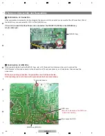
Page 40: ...l be activated After repairing be sure to remove the ground wire before reassembling Main capacitor GND MAIN Assy SIDE B Tuner pack chassis D MAIN Assy GND wire Be sure to disconnect the GND wire before reassembly After completion of reassembly before plugging the power cord into an outlet make sure that the 4P wires from CN5 of the MAIN Assy are connected to CP104 of the D MAIN Assy If the unit i...

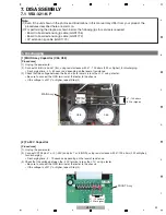
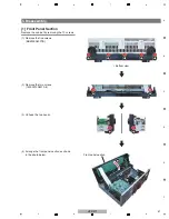
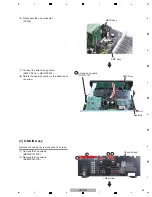
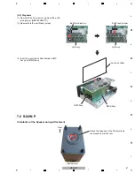
Page 41: ... the cabinet by removing the 10 screws 1 Remove the five screws BBZ30P080FTB 2 Remove the two screws 1500001206010 IL 3 Unhook the two hooks 4 Arrange the front panel section as shown in the photo below 1 1 1 1 1 2 3 3 2 4 Bottom view Front panel section 3 Disassembly ...

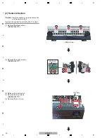
Page 42: ...ews Caution Heatsink section in work becomes hot and be careful with it 1 Remove the three screws BBZ30P080FTC 2 Remove the seven screws BBZ30P080FTC 3 Release the five binders 4 Remove the two screws BBZ30P080FTC 5 Remove the G H Assy 1 1 1 2 2 2 4 4 2 2 2 2 Bottom view G H Assy G L Assy 5 3 3 3 3 3 ...

Page 43: ... MAIN CP404 8 Rotate the heatsink section in the direction of the arrow MAIN Assy AMP Assy AMP Assy Heatsink 7 8 CP404 Extension jig cable GGD1773 6 3 D MAIN Assy Remove the cabinet by removing the 10 screws 1 Remove the five screws BBT30P100FTB 2 Remove the five screws BSZ30P040FTB Rear view Chassis back 1 1 1 1 1 2 5 ...

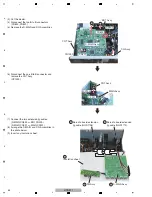
Page 44: ... D MAIN Assy BR1 Assy DG Assy DG Assy D MAIN Assy CNT Assy CNT Assy MAIN Assy 3 5 5 6 4 4 CN1000 CP1000 CP201 CN601 CN600 CN209 7 Connect the two extension jig cables D MAIN CN600 BR1 CN209 D MAIN CN601 MAIN CP201 8 Arrange the D MAIN and DG Assemblies in the photo below 9 Insert any insulation sheet Insulation sheet 7 Borad to board extension jig cable GGD1772 8 8 9 7 Borad to board extension jig...

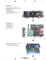
Page 45: ...Remove the chassis back Rear view Chassis back 1 1 2 2 1 1 1 1 1 1 1 4 2 MAIN Assy 1 Remove the three screws BBZ30P180FTC 2 Remove the six screws BBZ30P080FTC 3 Cut the four binders 4 Remove the G T Assy 1 1 1 3 3 3 3 2 2 2 2 2 2 MAIN Assy G T Assy 4 3 5 Arrange the unit as shown in the photo below 6 Connect the chassis ground See 2 Notes on Disassembly and Reassembly Confirmation of GND Wire 5 6 ...

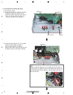
Page 46: ...Support Main chassis 1 2 2 2 2 MAIN Assy Screwdriver 3 Attach the three regulator ICs and a rectifier diode to the holes tapped in Step 2 Be sure to place them in a direction perpendicular to the board and take care that the jumper wires will not become distorted Note While securing the regulator ICs and rectifier diode to the holes for temporary joining tighten the screws while holding the regula...

Page 47: ...080FTC 2 Reassemble the earth lead jumper G H Assy Earth lead jumper Earth lead jumper G H Assy MAIN Assy AMP Assy 1 2 3 Insert any insulation sheet between AMP Assy and MAIN Assy 3 Insulation sheet Attach the speaker so that the terminals are placed nearer the rear Bottom view Rear Orientation of the Speaker during Attachment ...

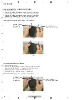
Page 48: ...nit face its terminal leftward Use other fingers to support the Cabinet front Use other fingers to support the Cabinet front Removing the FRONT SURROUND SPEAKER Fig 1 Fig 2 Use other fingers to support the Cabinet front Use other fingers to support the Cabinet front Fig 3 1 Remove the eight screws 2 Press on the side of the grille with both thumbs and slide it in frontward direction of the speaker...

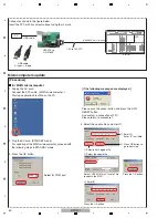
Page 49: ...M20812 Folder name EPConsole Folder name EPFlash_1_1_0_8 dotNetFx40_Full_setup exe 2 Install the driver Request the driver at the time of the conectting the Upgrade Jig and the PC with the USB cable Install the Driver CDM20812 3 Install NET Framework 3 0 service pack1 To work EPFlash exe application for rewriting the HDMI u co request to be installed the NET Framework 3 0 service pack1 on the PC F...

Page 50: ... the OK button if the following messages are displayed Please push the cancel button and press the JIG s RESET button And confirm a connection of FFC Please return to procedure 1 2 Plug the AC cord STANDBY mode For updating of the MAIN microcomputer proceed with the following steps in STANDBY mode 10P to 10P FFC Select for COM port 4 Select the update file and enter ID 1 Selection of upgrade file ...

Page 51: ...he Board rate then press the OK button 2 Update the MCU E P R Erase Program Read 2 Update the MCU Press the E P R button 1 Set speed of update 1 Set speed of update Press OK button If the following messages are displayed shut the update program down and start the update again from step 1 for HDMI SUB microcomputer 8 Unplug the AC cord Start up the application EPFlash on the PC 9 Select HDMI UP on ...

Page 52: ...isplayed shut the update program down and start the update again from step 8 11 Select the update file Press the OpenFile button 12 Press the START button to update the firmware 14 Turn the unit off STANDBY mode and unplug the AC cord Disconnect the FFC cable 15 Unplug the AC cord Start up the application EPConsole on the PC 16 Select CEC UP on the Upgrade Jig Connect the PC and the Upgrade Jig Co...

Page 53: ...act switch of the Upgrade Jig press STANDBY ON button After 2 or 3seconds release the tact switch button 24 Turn the unit off 23 Make sure that the main unit is in STANDBY mode Press and hold the ENTER and STANDBY ON keys then press the ENTER key to display each UCOM version Each time the ENTER key is pressed then indications on the FL display change as follows If the following messages are displa...

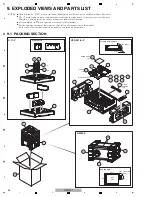
Page 54: ...en replacing be sure to use parts of identical designation Screws adjacent to b mark on product are used for disassembly For the applying amount of lubricants or glue follow the instructions in this manual In the case of no amount instructions apply as you think it appropriate SET Side Top Front Poly bag Style Tape 100 x 180 Clear Tape Clear Power cord Poly bag Packing Style Poly bag Style SYXE8 D...

Page 55: ...6327040059000 IL 24 Band Packing 8952SHM700046 IL 25 Box Gift See Contrast table 2 26 Packing Top S 11 P 8952S11005541 IL 27 Packing Top S 11 P 8952S11005542 IL 28 Packing S 22W P 8952S22W05191 IL Mark No Description Part No Mark No Symbol and Description HTP 071 SYXE8 HTP 071 CXE HTP 071 DLPWXE HTP 071 AXE5 1 Power Cord L068250160020 IL Not used L068250100080 IL Not used 5 S 22W Total Assy 8952S2...

Page 56: ...56 HTP 071 1 2 3 4 A B C D E F 1 2 3 4 9 2 VSX 321 K P SECTION L N F G H DLPWXE only Cushion EVA Nut Nut ...

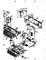
Page 57: ...57 HTP 071 5 6 7 8 5 6 7 8 A B C D E F A B C D J K N M I E Silicon grease GEM1057 Silicon adhesive GYA1011 for SYXE8 DLPWXE 23 for CXE AXE5 A Heatsink ...

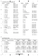
Page 58: ...321L 5077213123200 IL 42 Knob 5080212431000 IL 43 Button 5090213741100 IL 44 5 Key Button 5090214561000 IL 45 10 Key Button 5090214571000 IL 46 Cover See Contrast table 2 47 Cover See Contrast table 2 48 49 50 Screw BBT30P100FTB 51 Screw BBT40P080FTB 52 Screw BBZ30P080FTB 53 Screw BBZ30P080FTC 54 Screw BBZ30P180FTC 55 Screw BSZ30P040FTB 56 Screw Tapping Assy B018230141H11 IL 57 Screw Tap Tite B020...

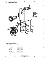
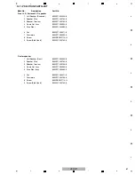
Page 59: ...T Mark No Description Part No 1 Unit Assy 8952S22W00009 IL 2 Network Assy 8952S22W00011 IL 3 Speaker Terminal 8952S22W00004 IL 4 Foot Mold 8952S22W00007 IL 5 Foot Cushoin 8952S22W00200 IL 6 Cashmere 8952S22W00210 IL 7 Screw Bind Head 8952SHM700039 IL 8 Screw Bind Head 8952S21W05381 IL ...

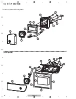
Page 60: ...60 HTP 071 1 2 3 4 A B C D E F 1 2 3 4 9 4 S 11 P SECTION Center speaker Front L R Surround L R speaker ...

Page 61: ...S11005350 IL 5 Case Rear 8952S11005380 IL 6 Felt 8952S11005411 IL 7 Cassimere 8952S11005430 IL 8 Screw 8952SB3001110 IL 9 Screw Bind Head 8952S11005150 IL Center speaker 1 Unit Speaker Front 8952S11005090 IL 2 Speaker Wire 8952S11005140 IL 3 Speaker Terminal 8952S11005100 IL 4 Frame Net Assy 8952S11005030 IL 5 Case Rear Assy 8952S11005060 IL 6 Felt 8952S11005411 IL 7 Cassimere 8952S11005130 IL 8 S...

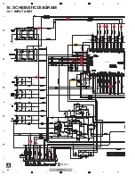
Page 62: ...76 10K R468 10K Q415 INC2001AC1 R473 R466 4 3 2 1 IC403 1 2 AZ4580 5 6 7 8 IC403 2 2 AZ4580 R516 0 R576 10K C512 3N3 K R549 100K R561 10K R477 470K R560 10K C509 10 50 R562 C473 10N K R483 470K R479 470K R447 4K7 C546 330P J C547 330P J C503 Q425 2SK117Y C516 1 50 C425 150N R 63V R555 470K R587 470K R547 470K C428 100 16 C429 100 16 R591 470K R594 470K R578 470K C431 100 16 R481 470K C434 10 50 C4...

Page 63: ...406 KDS4148U D404 KDS4148U LUG007 R585 1K R584 1K R579 1K Q421 RT1P141C R526 0 R501 470K Q419 RT1P141C R449 47K C474 10 50 R444 470 R436 47K R433 470 R421 47K R427 470 R410 47K C432 100 16 D402 KDS4148U D410 KDS4148U R581 1K Q420 RT1P141C R464 47K R415 470 CN400 2 0MM 12P 3 6 4 7 5 1 2 10 12 8 11 9 23 22 20 19 21 16 18 17 15 13 14 CP400 C125Z2 23 98 97 96 95 94 93 92 91 90 89 88 87 86 85 84 4 3 2 ...

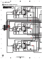
Page 64: ... R222SL 0R47 2 R225SW 330K R226SW 75K R224SW 27K D201SL 1SS133T R226SR 75K R224SR 27K R225SR 330K Q207SW KTC3200BL R227SL 2K2 Q207SR KTC3200BL Q203SW KTC3200BL R206SW 33K Q201SW KSA992F C205SW 100 10 C201SW 10 50 470K R205SW R210SL 470 R209SL 1K2 R207SL 1K5 470K R2056SL C204SL 33P 500V Q203SR KTC3200BL C205SR 100 10 Q201SR KSA992F R206SR 33K C201SR 10 50 470K R205SR R219SW 47 1 4 R221SW 0R47 2 R22...

Page 65: ... Q206C R220C 0R47 2 R221C 0R47 2 R219FR 47 1 4 C209FR 100P 500V R226C 75K C211C 22N R225FL 330K R226FL 75K R221FR 0R47 2 C211FR 22N Q208 KTA1268BL C215 4 7 50 C213 330 6 3 6 3 11 C214 10 50 C216 330 6 3 6 3 11 CP202 2SB1560Y Q206FL R230FR 22K R230FL 22K R230SL 22K R230SW 22K CN203 R204C 33K C201C 10 50 Q201C KSA992F R203C 7K5 R204FL 33K C201FL 10 50 Q201FL KSA992F R203FL 7K5 C202FR 680P C210C 100P...

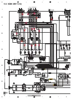
Page 66: ... 47N EB 100V C19 47N EB 100V C16 47N EB 100V C94 10N K R80 0R1 5 L1SW SP 2507 C88 100 16 6 3 11 C90 100 6 3 6 3 5 R90 4K7 R28 2K2 1 R29 2K2 1 R23 10 R92 2K2 C57 10 50 1 2 3 4 CN5 5267 04A C112 10N K R22 10 C62 FROM MAIN TRANS TO CHASSIS TO CHASSIS C115 10N K C81 47N EB 100V C84 4700 25 16 31 5 C85 1000 25 10 20 R31 0R22 1 C74 10N K C67 100N R 250V C61 100N EB 100V R9 10 1 RLY1 C5 2N2 K C10 2N2 K J...

Page 67: ... Q603 1 2 3 4 5 6 8 7 9 PACK601 C628 JACK3 C115 10N K R60 27K C34 47 16 R6 R89 3K6 Q20 KTC3198Y ZD10 MTZ3 3B Q9 RT1N237C RT1N237C Q11 RT1N237C Q12 R43 R50 51K R49 51K C103 1 50 C101 330 63 12 5 20 RT1N237C Q8 1 3 2 CP4 5267 03A R93 22K Q14 KTC3198Y C635 BEAD601 BD3580 R608L 1K R5 75 C35 47N Z R3 0 R627 R628 C627 D29 1SS133T D8 1SS133T R73 Q2 RT1P237C Q4 RT1P237C Q5 RT1P237C C60 R58 27K R64 22 1 4 ...

Page 68: ...22 R268 10K R243 3K3 Q201 ISA1530AC1 R281 4K7 R231 C225 10N K C226 47 16 C228 10N K R235 10K R301 47K 1 2 3 4 5 6 7 8 IC204 CW24C16DR R309 22 C220 10N K C216 R320 22 C214 R310 22 R269 R257 4K7 C241 C208 100N K D203 KDS4148U D202 KDS4148U R265 220K R249 1K R256 4K7 Q202 RT1N237C R236 10K R272 100K D206 KDS4148U D207 KDS4148U C217 100 10 C243 100N K RES201 16M9344 16P R213 47K 3 2 1 4 5 11 9 12 8 13...

Page 69: ...00N K 100N K D311 1SS133T D205 0 R264 10K R263 1K 100N K 10N K C222 100P J 1 3 2 CP404 20010WS 03 C220 10N K C216 R269 Q217 KTA1504S Q210 2SC3052 C249 10P D R219 C247 1N K R302 47K R327 47K 10N K 10N K 100N K 1 19 17 15 7 9 11 13 5 3 18 16 14 6 10 4 12 8 2 20 21 24 26 22 23 25 27 1 25 2 27P C241 C232 10N K R272 100K D206 KDS4148U D207 KDS4148U C217 100 10 C243 100N K RES201 16M9344 16P R222 R221 R...

Page 70: ...289 R293 10K D239 CDS2C05HDMI1 D231 CDS2C05HDMI1 D235 CDS2C05HDMI1 D238 CDS2C05HDMI1 D230 CDS2C05HDMI1 D234 CDS2C05HDMI1 D233 CDS2C05HDMI1 D237 CDS2C05HDMI1 D229 CDS2C05HDMI1 D273 CDS2C05HDMI1 D274 CDS2C05HDMI1 D275 CDS2C05HDMI1 D243 CDS2C05HDMI1 D247 CDS2C05HDMI1 D242 CDS2C05HDMI1 D246 CDS2C05HDMI1 D241 CDS2C05HDMI1 D245 CDS2C05HDMI1 D244 CDS2C05HDMI1 D266 CDS2C05HDMI1 R212 1K C211 100N K C209 10...

Page 71: ...C207 NJM2831F33 R255 10K CB215 0 C236 IC205 IL1117 3 3 R278 0 R260 4R7 C267 100N K C266 100N K CDS2C05HDMI1 D257 CDS2C05HDMI1 D259 CDS2C05HDMI1 D255 CDS2C05HDMI1 D261 CDS2C05HDMI1 D263 1 3 5 7 9 11 13 15 17 18 2 4 6 8 10 12 14 16 19 JACK204 CB222 0 R330 100 CB208 VCC 41 R247 47K D265 UDZ5 1B C222 100N K R325 100 R246 2K2 R269 10K C233 47 16 Z8156 CB209 0 CB210 10 R329 100 R331 100 CB207 CB204 0 C2...

Page 72: ...20 16 Z8157 C611 10N K C696 10 25 Z8155 C613 10N K C614 1 50 Z8155 C698 220 6 3 Z8157 CN603 3 6 4 7 5 1 2 10 12 8 11 9 23 22 20 19 21 16 18 17 15 13 14 CN600 C125Z2 23 C673 X5R106 K 25V TDK D161 C624 10 16 Z8154 C601SBL 4N7 K C604SBL 470P J C601SBR 4N7 K C604SBR 470P J R601SW 560 C604SW 470P J C604C 470P J R601C 560 C601SL 4N7 K R601SL 560 R601SR 560 C601SR 4N7 K C601FL 4N7 K C601FR 4N7 K C604FL 4...

Page 73: ...00N K C609FR 10 16 Z8154 C640 10 16 Z8154 C641 68N K C642 100N K R629 680 R644 1M C673 X5R106 K 25V TDK R271 330 R303 4K7 R302 4K7 R311 0 R308 0 R306 0 R304 0 R674 C626 Z8154 C619 1N K R673 L160 15UH R321 100 R322 100 C635 4N7 K R270 330 C645 100N K L148 0 R312 0 R307 0 R305 0 R313 0 R314 0 R647 L141 LBC2012T 4 7UH C618 1N K C651 10 16 Z8154 C639 10 16 Z8154 C644 100N K L147 0 28 27 1 26 25 24 23 ...

Page 74: ...R727 33 R725 33 C509 R741 1K C515 100P J C516 100P J R752 0 R755 0 R751 33 R754 33 R756 33 R760 33 R709 33 C460 10N K C461 220 6 3 Z8157 C465 220 6 3 Z8157 C467 100 6 3 Z8156 C468 C472 10N K C476 100P J C483 CH1N J C473 100N K C480 330P J C482 100N K C478 100P J C479 1N K C475 1N K C477 100N K C487 330P J C491 10N K C498 10N K C488 100N K C495 10N K C492 100N K C494 100N K C499 100N K C502 C506 R7...

Page 75: ... 53 52 5 4 6 7 8 9 10 11 12 13 14 15 16 41 42 43 44 45 46 47 48 49 50 51 39 40 33 34 35 36 37 38 29 30 31 32 28 17 18 19 20 21 22 23 24 25 26 27 IC103 IS42S16400F 6TL R810 33 R808 33 R804 33 R803 33 R800 33 R799 33 R797 33 R791 33 R790 33 R788 33 R758 33 C523 10N K L154 0 C520 R811 33 C518 330P J R805 33 R809 33 R802 33 R801 33 R798 33 R794 33 R796 33 R795 33 R792 33 R789 33 R787 33 C524 10P D C52...

Page 76: ...Y_KEY PDN CPU 3 3V HDMI 12V C757 820P K D711 KDS4148U D709 KDS4148U C250FR 10P D C250SBL 10P D C250C 10P D CN702 3 6 4 7 5 1 2 10 12 8 11 9 23 22 20 19 21 16 18 17 15 13 14 CN210 C125Z1 23 C744 10N K 3 6 4 7 5 1 2 10 12 8 11 9 23 22 20 19 21 16 18 17 15 13 14 CN209 C125Z1 23 E F G H E BR1 ASSY 7028071133010 IL F HP ASSY 7028071134010 IL G FUNC ASSY 7028071132010 IL A CP400 N CP701 C 1 2 CP5 D 2 3 ...

Page 77: ...766 R778 10K C710 C708 C706 C724 C729 C712 C713 C714 C715 C716 C725 10N K CN701 270MM 9P R788 OSD FLT_DATA C728 10 50 KEY1 STBY_KEY C719 47N EB 100V C727 10N K C730 1 50 R707 56K R706 56K R708 56K R710 56K R709 56K R705 56K R712 56K R714 56K R716 56K R718 56K R720 56K R723 56K R724 56K R726 56K R728 56K R725 56K C717 1 50 C718 47N EB 100V R732 56K R730 56K STBY_RLY CPU_ST_VCC GNDU C739 1N K C741 1...

Page 78: ...1 2 3 4 10 9 DG ASSY C603 47 16 R615 0 JACK601 R612 10K C602 C601 10N K R610 4K7 R616 0 MT601 MT602 2 1 3 9 7 5 8 10 6 4 FPC202 1 0 11S 10PW R613 0 R614 0 C604 22P J L601 LBC2012T 4 7UH CP603 I I DG ASSY 7028071112010 IL D 2 3 CN603 ...

Page 79: ...21T BD1008 BD121T BD1006 BD121T BD1005 BD121T BD1002 BD121T BD1003 BD121T BD1001 BD121T CLAMP906 CLAMP_WIRE CLAMP907 CLAMP_WIRE CLAMP904 CLAMP_WIRE CLAMP903 CLAMP_WIRE M L K J J CNT ASSY 7028071151010 IL K G T ASSY 7028071123010 IL L G L ASSY 7028071125010 IL M G H ASSY 7028071124010 IL C 2 2 CP201 D 2 3 CN601 ...

Page 80: ...09 KDS4148U ZD302 MTZ15B IC301 IL1117 3 3 1 3 2 CP303 1 3 2 CP304 5267 03A 220V AXE5 230V SYXE8 120V CXE CXE ONLY 220 240V DLPWXE J302 J301 2 1 CP302 35328 0263 C304 4N7 GND302 C305 100N K Q302 RT1N144C Q303 2SC3052 ZD303 MTZJ7 5B 2 1 PT301 D302 KDS4148U D310 KDS4148U 1 2 3 4 5 6 8 7 9 CP701 20010WR 09 N STBY ASSY SYXE8 7028071122040 IL CXE 7028071122030 IL DLPWXE 7028071122020 IL AXE5 70280711220...

Page 81: ...nce temperature characteristics If an abnormal current flows to P SW due to an excessive input or unusual signal P SW heats up and the resistance rapidly increases With this function the speakers are protected from excessive input or unusual signal The resistance value increases even when using a soldering iron for repairing so allow it to cool before using ...

Page 82: ...E F 1 2 3 4 11 PCB CONNECTION DIAGRAM 11 1 INPUT ASSY A A INPUT ASSY SIDE A B CP201 E CN210 CP400 C CP17 CP401 CN400 Q408 Q409 Q412 Q415 Q402 Q405 Q406 Q427 Q426 Q420 Q421 Q419 Q407 Q410 IC403 IC402 Q413 Q417 IC400 Q411 Q414 Q416 ...

Page 83: ...NOTE FOR PCB DIAGRAMS 1 The parts mounted on this PCB include all necessary parts for several destinations For further information for respective desti nations be sure to check with the sche matic diagram Capacitor Connector P C Board Chip Part SIDE A SIDE B 2 View point of PCB diagrams ...

Page 84: ... AMP ASSY B AMP ASSY SIDE A SIDE B A CN400 C CN CP203 CP203 CP201 C CN3 CP202 CP201 CP202 C CP404 CN203 CN203 Q208 Q207FR Q207SR Q205SR Q204SR Q206SR Q203FR Q202FR Q202SR Q203SR Q207C Q202C Q201C Q203C Q2 Q205C Q204C Q206C Q201SR Q201FR Q205FR Q204FR Q206FR ...

Page 85: ...7 8 A B C D E F B SIDE A SIDE B A CN400 C CN1 CP203 CP203 CP201 CP201 2 Q207SW Q202SW Q201SW Q203SW Q207SL Q202SL Q201SL Q203SL Q204SL Q206SL Q205FL Q204FL Q206FL Q207FL Q202FL Q201FL Q203FL Q205SW Q204SW Q206SW Q205SL Q206C ...

Page 86: ...86 HTP 071 1 2 3 4 A B C D E F 1 2 3 4 11 3 MAIN ASSY C C MAIN ASSY SIDE A F CN721 MAIN TRANS CP1 MAIN TRANS CP3 CP5 B CP203 CN1 B CP202 CN3 Q18 Q19 ...

Page 87: ...87 HTP 071 5 6 7 8 5 6 7 8 A B C D E F C SIDE A MAIN TRANS CP2 MAIN TRANS CP3 D CP104 CN5 B CN203 CP404 J CP1000 CP201 H CN704 CN704B A CP401 CP17 Q17 Q14 Q15 Q16 Q21 Q20 IC2 IC1 IC3 ...

Page 88: ...88 HTP 071 1 2 3 4 A B C D E F 1 2 3 4 C C MAIN ASSY SIDE B CP2 CP3 CN5 CP404 CP201 CN704B CP17 IC4 Q603 Q202 Q201 Q2 Q1 Q5 Q4 Q11 Q215 Q209 Q212 Q217 Q216 Q211 Q206 Q203 Q210 Q12 Q8 Q9 Q602 IC203 IC204 ...

Page 89: ...89 HTP 071 5 6 7 8 5 6 7 8 A B C D E F C SIDE B CP1 CP3 CP5 CN1 CN3 ...

Page 90: ...90 HTP 071 1 2 3 4 A B C D E F 1 2 3 4 11 4 D MAIN ASSY D D D MAIN ASSY SIDE A E CN209 CN600 C CN5 CP104 ...

Page 91: ...91 HTP 071 5 6 7 8 5 6 7 8 A B C D E F D SIDE A J CN1000 CN601 I CP603 CN603 IC609 IC600 IC602 IC601 IC100 IC608 IC607 IC103 IC207 IC201 Q204 Q208 IC203 IC102 IC206 IC200 IC205 IC202 IC101 ...

Page 92: ...92 HTP 071 1 2 3 4 A B C D E F 1 2 3 4 D D D MAIN ASSY SIDE B CN601 CN603 IC104 IC603 IC604 IC605 IC606 ...

Page 93: ...93 HTP 071 5 6 7 8 5 6 7 8 A B C D E F D SIDE B CN600 CP104 ...

Page 94: ...5 BR1 HP FUNC and FRONT ASSYS E BR1 ASSY E BR1 ASSY G FUNC ASSY G FUNC ASSY F HP ASSY F HP ASSY SIDE A SIDE B D CN600 CN209 CN209 A CP400 CN210 CN210 N CP701 CN701 CN701 C CP5 CN721 CN721 CP702 CP702 CN702 CN702 Q702 Q701 Q703 Q707 Q705 E F G H ...

Page 95: ...95 HTP 071 5 6 7 8 5 6 7 8 A B C D E F H FRONT ASSY H FRONT ASSY SIDE A SIDE B C CN704B CN704 CN704 IC701 Q706 Q708 Q704 Q709 RMC701 H ...

Page 96: ...96 HTP 071 1 2 3 4 A B C D E F 1 2 3 4 11 6 DG ASSY I DG ASSY I DG ASSY SIDE A SIDE A SIDE B SIDE B I D CN603 CP603 CP603 ...

Page 97: ...97 HTP 071 5 6 7 8 5 6 7 8 A B C D E F 11 7 CNT ASSY J CNT ASSY J CNT ASSY SIDE A SIDE A SIDE B SIDE B J C CP201 CP1000 D CN601 CN1000 CP1000 CN1000 ...

Page 98: ...98 HTP 071 1 2 3 4 A B C D E F 1 2 3 4 11 8 G T G L and G H ASSYS M G H ASSY M G H ASSY K G T ASSY L G L ASSY K G T ASSY L G L ASSY SIDE A SIDE A SIDE B SIDE B M L K ...

Page 99: ...P 071 5 6 7 8 5 6 7 8 A B C D E F 11 9 STBY ASSY N STBY ASSY N STBY ASSY SIDE A SIDE A SIDE B SIDE B N CP302 CP302 H CN700 CP701 CP701 MAIN TRANS MAIN TRANS CP301 CP301 AC IN CP304 CP304 Q303 Q301 Q302 IC301 ...

Page 100: ... CN BEAD L F FU FLT V JACK JA JACK JA9 JK JA PT T REG IC REG IC9 RLY RY RMC U RES X XTAL X9 BD L7 LED D8 Z D9 ZD D9 DZ D9 SW S VEC S9 GND KN SCHEMATIC DIAGRAM and PCB CONNECTION DIAGRAM PCB PARTS LIST Mark No Description Part No LIST OF ASSEMBLIES NSP 1 PCB TTL ASSY FRONT 7025HK1103011 IL 2 FRONT ASSY 7028071131010 IL 2 FUNCT ASSY 7028071132010 IL 2 BR1 ASSY 7028071133010 IL 2 HP ASSY 702807113401...

Page 101: ...SSY SEMICONDUCTORS Q 201 202 J5000992F0050 IL Q 203 207 J5023200B0050 IL Q 208 J5001268B0050 IL D 201 202 K000013300520 IL D 208 J5001268B0050 IL MISCELLANEOUS CN203 CN WIRE L002800030110 IL CN9201 CN WAFER 2 0MM L101200101210 IL CN9202 CN WAFER 2 0MM L101200100810 IL CN9203 CONNECTOR 6P L102526700600 IL RESISTORS R 211 218 219 C060047063050 IL R 216 217 C060056265050 IL R 220 223 C060R47066050 IL...

Page 102: ...0 IL D 209 211 213 215 K067020500010 IL D 217 219 221 223 K067020500010 IL D 225 227 229 231 K067020500010 IL D 233 235 237 239 K067020500010 IL D 241 247 252 264 K067020500010 IL D 248 250 265 UDZS5R1 B Mark No Description Part No D 251 K005041480030 IL D 266 276 K067020500010 IL MISCELLANEOUS L 141 153 COIL INDUCTOR D3104R7010200 IL L 160 COIL CHIP D311126000030 IL JA 201 204 CN WAFER L109100190...

Page 103: ...rvice parts M G H ASSY MISCELLANEOUS 903 907 JHMX9800 ON HAITI 4330000120000 IL N STBY ASSY SEMICONDUCTORS IC 301 J126111700041 IL Q 301 303 J522305200050 IL D 301 302 309 310 K005041480030 IL D 303 304 K005041480030 IL D 305 308 K000400700010 IL D 9301 UDZS5R1 B D 9303 UDZS7R5 B MISCELLANEOUS H 301 9301 HOLDER FUSE CLIP G645000050010 IL RY301 RELAY G680060102020 IL T 301 POWER TRANS 8200280150680...

Reviews: