28
DEH-3300R-2,3330R-2
Pin No.
Pin Name
I/O
Function and Operation
58-61
FLGA-D
O
External flag output terminal for internal signal monitor
62
VDD
D power supply terminal (5 V)
63
VSS
Digital ground terminal
64
IO0
O
RF amplifier gain switching terminal
65
IO1
O
Not used
66
IO2
I
HOME detection switch input terminal
67
IO3
O
FocusDrv and signal output terminal
68
dmout
I
Field equalizer PWM output terminal for IO0 and IO1
Disc equalizer PWM output terminal for IO2 and IO3
69
ckse
I
Usually open
70
dact
I
DAC test mode terminal
71
TESIN
I
Test input terminal
72
TESIO1
I
Test input/output terminal
73
VSS
Digital ground terminal
74
PXI
I
DPS-system clock oscillator circuit input terminal
75
PXO
O
DPS-system clock oscillator circuit output terminal
76
VDD
D power supply terminal (5 V)
77
XVSS
Ground terminal for system clock oscillator circuit
78
XI
I
System clock oscillator circuit input terminal
79
XO
O
System clock oscillator circuit output terminal
80
XVDD
For system clock oscillator c power supply terminal
81
DVSR
R channel D/A converting unit power supply terminal
82
RO
O
R channel data forward rotation output terminal
83
DVDD
D/A converting unit power supply terminal (5 V)
84
DVR
Reference voltage terminal
85
LO
O
L channel forward rotation output terminal
86
DVSL
L channel D/A converting unit power supply terminal
87-89
TEST1-3
I
Test mode terminal
90-93
BUS0-3
I/O
Data input/output terminal for microcomputer interface
94
VDD
D power supply terminal (5 V)
95
VSS
Digital ground terminal
96
BUCK
I
Clock terminal for microcomputer interface
97
cee
I
Chip enable signal for microcomputer interface
98
TEST4
I
Test mode terminal
99
tsmod
I
Test mode terminal
100
rst
I
Reset signal input terminal
30
31
50
51
80
81
100
1
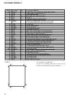
*TC9495F2
IC's marked by* are MOS type.
Be careful in handling them because they are very
liable to be damaged by electrostatic induction.


