background image


PDP-433PU

5

5

6

7

8

5

6

7

8

C

D

F

A

B

E

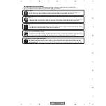
[ Important symbols for good services ]

In this manual, the symbols shown-below indicate that adjustments, settings or cleaning should be made securely.
When you find the procedures bearing any of the symbols, be sure to fulfill them:

2. Adjustments

To keep the original performances of the product, optimum adjustments or specification confirmation is indispensable. 
 In accordance with the procedures or instructions described in this manual, adjustments should be performed.

3. Cleaning

For optical pickups, tape-deck heads, lenses and mirrors used in projection monitors, and other parts requiring cleaning,
proper cleaning should be performed to restore their performances. 

5. Lubricants, glues, and replacement parts

Appropriately applying grease or glue can maintain the product performances. But improper lubrication or applying 
glue may lead to failures or troubles in the product. By following the instructions in this manual, be sure to apply the
prescribed grease or glue to proper portions by the appropriate amount.For replacement parts or tools, the prescribed 
ones should be used.

4. Shipping mode and shipping screws

To protect the product from damages or failures that may be caused during transit, the shipping mode should be set or
the shipping screws should be installed before shipping out in accordance with this manual, if necessary.

1. Product safety

You should conform to the regulations governing the product (safety, radio and noise, and other regulations), and 
should keep the safety during servicing by following the safety instructions described in this manual.    

Summary of Contents for ARP3184

Page 1: ...PIONEER CORPORATION 2003 ARP3184 T ZZY NOV 2003 Printed in Japan THIS MANUAL IS APPLICABLE TO THE FOLLOWING MODEL S AND TYPE S Model PDP 434PG Type Power Requirement Remarks TLDFR PDP 434PG AC110 240V PLASMA DISPLAY This service manual should be used together with the following manual s Model No Order No Remarks PDP 434PE WYVI6 ARP3174 SAFETY INFORMATION EXPLODED VIEWS AND PARTS LIST BLOCK DIAGRAM...

Page 2: ... effective digits any digit apart from 0 such as 560 ohm and 47k ohm tolerance is shown by J 5 and K 10 Ex 2 When there are 3 effective digits such as in high precision metal film resistors 5 6 1 4 7 3 R 5 0 1 R 0 5 6 2 1 560 47k 0 5 1 RD1 4PU J RD1 4PU J RN2H K RS1P K 56 x 101 47 x 103 R50 1R0 561 473 5 62k RN1 4PC F 562 x 101 5621 PDP 434PG TLDFR and PDP 434PE WYVI6 are constructed the same exce...

Page 3: ...ogether with the following manual s This product is component of system Model Type Power Requirement Remarks PDP 433PU KUC AC120V PDP 433PE WYVI6 AC220 240V PDP 433PE WYVI6XK AC220 240V PDP 433PG TLDPKBR AC110 240V Model No Order No Remarks PDP 433PU PDP 433PE PDP 433PG ARP3144 SCHEMATIC DIAGRAM and PCB DIAGRAM Component System Service Manual Remarks Plasma Display System PDP 4330HD PDP 433HDE PDP...

Page 4: ... adjustment and compartment covershields isolation resistor capacitor etc 3 When service is required observe the original lead dress Extra precaution should be taken to assure correct lead dress in the high voltage circuitry area 4 Always use the manufacture s replacement components Especially critical components as indicated on the circuit diagram should not be replaced by other manufacture s Fur...

Page 5: ... Any current measured must not exceed 0 5mA ANY MEASUREMENTS NOT WITHIN THE LIMITS OUTLINED ABOVE ARE INDICATIVE OF A POTENTIAL SHOCK HAZARD AND MUST BE CORRECTED BEFORE RETURNING THE SET TO THE CUSTOMER PRODUCT SAFETY NOTICE Many electrical and mechanical parts in PIONEER set have special safety related characteristics These are often not evident from visual inspection nor the protection afforded...

Page 6: ... SUPPLY Module 6 Other primary side of the SW POWER SUPPLY Module High Voltage Generating Point The places where voltage is 100V or more except for the charged places described above If the places are touched there is a risk of electric shock 1 SW POWER SUPPLY Module 215V 2 X DRIVE Assy 280V to 215V 3 Y DRIVE Assy 345V 4 SCAN A Assy 345V 5 SCAN B Assy 345V 6 X CONNECTOR A Assy 280V to 215V 7 X CON...

Page 7: ...es 5 Lubricants glues and replacement parts Appropriately applying grease or glue can maintain the product performances But improper lubrication or applying glue may lead to failures or troubles in the product By following the instructions in this manual be sure to apply the prescribed grease or glue to proper portions by the appropriate amount For replacement parts or tools the prescribed ones sh...

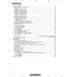
Page 8: ...DRIVE ASSY 39 3 1 5 Y DRIVE ASSY 40 3 1 6 SUB ADDRESS A and B ASSYS 42 3 1 7 ADR RESONANCE ASSY 43 3 1 8 ADR CONNECT A B C and D ASSYS 44 3 1 9 AUDIO AMP and SP TERMINAL ASSYS 45 3 2 WAVEFORMS 46 For SCHEMATIC DIAGRAM refer to ARP3144 4 PCB CONNECTION DIAGRAM Refer to ARP3144 5 PCB PARTS LIST 50 6 ADJUSTMENT 60 6 1 SERVICE FACTORY MODE 60 6 1 1 How to Enter the Service Factory Mode 61 6 1 2 Genera...

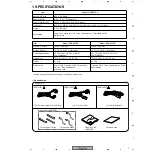
Page 9: ...W 0 6 W Standby Dimensions 1070 W 630 H 98 D mm 421 8 W 2413 16 H 37 8 D inch Weight 31 5 kg 69 4 lbs Accessories Power Cord Cleaning Cloth Three speed clamps Three bead bands Warranty card Item Model PDP 433PE Number of Pixels 1024 x 768 pixels Audio Amplifier 12 W 12 W 10 distortion Power Requirement AC 220 240 V 50 60 Hz 320 W 0 6 W Standby Dimensions 1070 W 630 H 98 D mm Weight 31 5 kg Accesso...

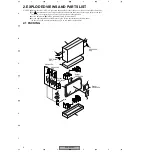
Page 10: ...t Therefore when replacing be sure to use parts of identical designation Screws adjacent to mark on product are used for disassembly For the applying amount of lubricants or glue follow the instructions in this manual In the case of no amount instructions apply as you think it appropriate NOTES 1 2 3 7 9 17 13 14 PDP 433PE Only PDP 433PU Only PDP 433PG Only Except PDP 433PU Except PDP 433PG Except...

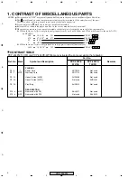
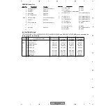
Page 11: ... Contrast table 2 17 Power Cord See Contrast table 2 18 Caution Sheet See Contrast table 2 19 Ferrite Core See Contrast table 2 20 Label Blue 16 AAX2787 21 Label Green 16 AAX2956 22 MIC Label See Contrast table 2 23 SP Spacer AEC1925 Mark No Description Part No Mark No Symbol and Description PDP 433PU KUC PDP 433PE WYVI6 PDP 433PE WYVI6XK PDP 433PG TLDPKBR 1 Packing Case 43 AHD3115 AHD3114 AHD3138...

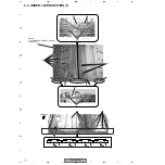
Page 12: ...PDP 433PU 10 1 2 3 4 1 2 3 4 C D F A B E 2 2 UNDER LAYER SECTION 1 9 13 1 10 10 3 2 2 or 3 12 Refer to 2 14 PANEL CHASSIS 43 ASSY AWU1067 14 14 8 8 Upper side 4 13 13 13 13 5 6 7 11 10 8 ...

Page 13: ...WZ6730 3 BRIDGE D Assy AWZ6731 NSP 4 ADR CONNECT A Assy AWZ6678 NSP 5 ADR CONNECT B Assy AWZ6679 NSP 6 ADR CONNECT C Assy AWZ6680 NSP 7 ADR CONNECT D Assy AWZ6681 8 Wire Saddle AEC1904 NSP 9 Panel Chassis 43 Assy AWU1067 10 Circuit Board Spacer AEC1872 NSP 11 PCB Spacer AEC1121 12 Circuit Board Spacer AEC1873 13 Screw VBB30P100FNI 14 Screw ABA1301 ...

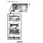
Page 14: ...PDP 433PU 12 1 2 3 4 1 2 3 4 C D F A B E 2 3 UNDER LAYER SECTION 2 11 11 Upper side 1 13 13 8 9 10 9 8 13 Upper side 2 17 12 12 18 17 3 14 14 14 14 4 5 6 14 14 16 7 14 15 Upper side 16 ...

Page 15: ...Assy AWZ6679 NSP 5 ADR CONNECT C Assy AWZ6680 NSP 6 ADR CONNECT D ASSY AWZ6681 NSP 7 Drive Heatsink Assy ANH1598 NSP 8 Metal Fitting ANG2464 NSP 9 Heat Sink ANH1594 10 Silicone Sheet AEH1039 11 Coil Silicon Sheet AEH1048 12 Circuit Board Spacer AEC1872 13 Screw ABZ30P060FMC 14 Screw VBB30P100FNI 15 Screw PMB30P060FNI 16 Drive Silicon Sheet AEH1041 17 Insulation Sheet A AEC1923 18 Insulation Sheet ...

Page 16: ...PDP 433PU 14 1 2 3 4 1 2 3 4 C D F A B E 2 4 UNDER LAYER SECTION 3 Upper side 8 8 3 4 8 9 1 Upper side Upper side 4 9 7 5 6 2 11 10 10 ...

Page 17: ...DRIVE Assy AWZ6749 2 Circuit Board Spacer AEC1872 NSP 3 Drive Heatsink Assy ANH1598 4 Drive Silicon Sheet AEH1041 5 Scan IC Spring 43L ABK1029 6 Scan IC Spring 43R ABK1030 7 Scan Insulation Sheet 43 AMR3287 8 Screw VBB30P100FNI 9 Screw PMB30P060FNI 10 Insulation Sheet A AEC1923 11 Insulation Sheet B AEC1924 ...

Page 18: ...PDP 433PU 16 1 2 3 4 1 2 3 4 C D F A B E 2 5 UNDER LAYER SECTION 4 Upper side 18 12 5 7 8 7 2 12 13 18 1 or 2 17 18 13 13 19 4 17 17 6 10 3 1 14 15 13 ...

Page 19: ...Z6729 3 SENSOR ASSY AWZ6696 4 ADR RESONANCE Assy AWZ6751 5 Brind Plate AMR3313 6 Insulation Sheet AMR3343 NSP 7 Heat Sink ANH1594 8 Silicone Sheet AEH1039 9 10 Rivet BEC1066 11 12 Metal Fitting ANG2464 13 Wire Saddle AEC1904 NSP 14 PCB Spacer AEC1121 15 Circuit Board Spacer AEC1873 16 17 Screw ABA1301 18 Screw ABZ30P060FMC 19 Screw VBB30P100FNI ...

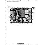
Page 20: ...1 D10 D16 D11 D15 D14 D13 D12 D17 SA1 SA2 X1 X2 TE1 SA2 SA1 D6 D7 D2 D3 D8 D9 K3 K3 Upper side 1 39 27 27 27 27 31 29 White Tape White Tape 16 2 10 27 30 36 5 3 4 17 43 33 38 18 1 39 39 21 22 23 27 24 2 3 4 14 13 12 37 35 15 27 27 8 11 5 9 19 27 32 6 7 41 28 34 20 27 40 42 25 26 ...

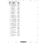
Page 21: ...WZ6727 19 X DRIVE Assy AWV1985 20 J204 Flexible Flat Cable ADD1207 21 J209 Flexible Flat Cable ADD1206 22 J210 Flexible Flat Cable ADD1204 23 J211 Flexible Flat Cable ADD1199 24 J212 Flexible Flat Cable ADD1201 25 J201 Flexible Flat Cable ADD1194 26 J202 Flexible Flat Cable ADD1194 27 Flat Clamp AEC1879 28 J203 Flexible Flat Cable ADD1198 29 J205 Flexible Flat Cable ADD1202 30 J206 Flexible Flat C...

Page 22: ...PDP 433PU 20 1 2 3 4 1 2 3 4 C D F A B E 2 7 MIDDLE LAYER SECTION 1 Upper side Upper side 12 11 6 11 11 1 7 5 3 2 12 2 Upper side Upper side 12 12 11 8 9 9 11 14 14 4 11 11 10 8 10 11 13 ...

Page 23: ...ANA1698 NSP 2 Card Spacer AEC1902 3 Niplocker AEC1803 4 Card Corner Holder BEC1144 5 Sub Frame L ANG2517 6 Sub Frame R ANG2518 NSP 7 Front Chassis HL 43 ANA1699 NSP 8 Front Chassis V 43 ANA1702 9 FPC Cushion 43 AEB1371 10 Insulation Sheet C AEC1927 11 Screw ABA1294 12 Screw BMZ30P060FMC 13 VR Cushion AEB1374 14 V Cushion AED1205 ...

Page 24: ...PDP 433PU 22 1 2 3 4 1 2 3 4 C D F A B E 2 8 MIDDLE LAYER SECTION 2 Upper side 9 10 27 7 8 5 6 29 29 29 14 14 8 16 16 16 14 28 11 8 13 12 15 8 1 17 20 19 4 30 18 30 2 21 3 30 26 32 22 22 23 25 24 32 31 ...

Page 25: ...42 11 J214 3P Housing Wire ADX2735 12 S2 Power Switch ASG1089 13 Niplocker BEC1136 14 PCB Spacer AEC1570 15 J215 3P Housing Wire ADX2757 16 Spacer AEC1360 17 Audio Base ANA1687 18 Screw BMZ30P060FZK 19 V Cushion AED1205 20 J113 Wire PJ ADX2742 NSP 21 IR Holder ANG2494 22 Nylon Rivet AEC1671 23 S1 Power Switch ASG1082 24 J106 Wire PC ADX2827 25 J104 3P Housing Wire ADX2748 NSP 26 Switch Holder ANG2...

Page 26: ...11 10 3 J201 J202 14 13 13 S4001 CBIT_1 S4004 CBIT_0 PDP 433P PDP 433PU PDP 433PE PDP 433PG Set the slide switches in accordance with applicable model when replacing the MR INTERFACE Assy Note 1 When there is not S4004 set only S4001 Note 2 When there are not S4001 and S4004 setting is unnecessary Caution in the MR INTERFACE Assy Replacement ...

Page 27: ...TX1037 4 J201 Flexible Flat Cable ADD1194 5 J118 Wire P ADX2765 6 J111 14P Housing Wire ADX2730 7 L3 Toroidal Core ATX1042 8 J214 3P Housing Wire ADX2735 9 J104 3P Housing Wire ADX2748 10 Ferrite Core Holder AEC1818 11 J113 Wire PJ ADX2742 12 J202 Flexible Flat Cable ADD1194 13 Screw TBZ40P080FZK 14 Screw AMZ30P060FZK 15 Screw BBA1051 16 Screw PMZ26P080FZK 17 Screw ABA1294 ...

Page 28: ...PDP 433PU 26 1 2 3 4 1 2 3 4 C D F A B E 2 10 UPPER LAYER SECTION 2 15 14 15 6 5 7 8 SW101 100V 200V 3 P4 P7 P3 P5 P6 P2 P1 11 10 12 9 16 7 1 18 13 PDP 433PU Only 17 ...

Page 29: ...AC Inlet with Filter AKP1223 7 J105 Wire PB ADX2826 8 J114 Earth Wire ADX2709 9 SP TERMINAL Assy AWZ6688 10 J101 13P Housing Wire ADX2768 11 J118 Wire P ADX2765 12 J103 13P Housing Wire ADX2766 13 J102 Wire PE ADX2738 14 Screw PMB30P060FNI 15 Screw AMZ30P060FZK 16 Screw BPZ30P080FZK 17 Solder Warning Label See Contrast table 2 18 Screw BMZ30P060FZK Mark No Description Part No Mark No Symbol and De...

Page 30: ...PDP 433PU 28 1 2 3 4 1 2 3 4 C D F A B E 2 11 FRONT CASE SECTION Foil Side 2 3 13 6 7 7 12 12 5 4 7 8 7 12 9 9 11 10 10 12 12 7 19 18 12 7 8 8 8 1 16 15 17 PDP 433PU Only 20 21 ...

Page 31: ...519 8 Spacer AEC1896 9 Panel Cushion V 43 AED1201 10 Panel Cushion H 43 AED1200 11 Protect Panel Assy 43 AMR3303 12 Screw ABZ30P050FZK 13 Screw VMZ30P060FZK 14 15 Serial Seal AAX2609 16 J213 Flexible Flat Cable ADD1193 NSP 17 Flexible Seal P AEH1052 18 Power Button AAD4113 19 Coil Spring ABH1108 20 Energy Star Label See Contrast table 2 21 HDTV Label See Contrast table 2 Mark No Description Part N...

Page 32: ... Gray AAX2926 NSP 6 Name Label HD Gray See Contrast table 2 7 Bolt Caution Label Gray AAX2928 8 Terminal Display Label P Gray See Contrast table 2 9 Terminal Display Label L Gray See Contrast table 2 10 Label Blue 8 AAX2786 11 Label Green 8 AAX2955 12 MIC Label See Contrast table 2 Mark No Description Part No Mark No Symbol and Description PDP 433PU KUC PDP 433PE WYVI6 PDP 433PE WYVI6XK PDP 433PG ...

Page 33: ...acer AEC1872 Circuit Board Spacer AEC1873 Spacer AEC1896 NSP Card Spacer AEC1902 Wire Saddle AEC1904 Panel Cushion H 43 AED1200 Panel Cushion V 43 AED1201 V Cushion AED1205 Insullation Sheet AMR3263 Scan Sheet 43 AMR3287 Card Corner Holder BEC1144 Insulation Sheet C AEC1927 Panel Caution Sheet ARM1217 Brind Plate AMR3313 Insulation Sheet AMR3343 Screw ABA1283 Screw ABA1294 Screw ABZ30P060FMC Screw...

Page 34: ...r Coner Label AAX2862 2 Silicone Sheet 43 AEH1043 2 Adhesive Tape 43 AEH1044 2 Adhesive Tape B 43 AEH1054 2 Panel Silicone Sheet AEH1055 2 Silicone Sheet B43 AEH1056 Pin Grommet AEC1015 Scan Silicone Sheet AEH1058 NSP Plasma Panel Assy 43 AAV1239 Screw VBB30P100FNI Protection Tape AEH1059 Mark No Description Part No NSP 1 SCAN FUKUGO ASSY AWV1969 2 SCAN A ASSY AWZ6724 2 SCAN B ASSY AWZ6725 2 X CON...

Page 35: ...ess consumer models and module It is supplied by installing the Circuit Board Spacer AEC1872 and the Wire Saddle AEC1904 as follows Therefore it is necessary to remove them in accordance with the models Confirm the character of the seal carved near the parts and then remove them P for Consumer models only W for Module only PW Common use for Consumer models and Module In case of this unit 433PU 433...

Page 36: ...711 VADR Gen K2 K1 SAB3 SAB1 SAB2 VADR2 ADR_CO 60 IC5 VCC_VH PSUS VCP VC_VF VC_VF V_OFS VCC_VH V_IC5V V 3V_I V 3V V 3V_IC V 2V_IC V 2V_I V 5V_STB TXD RX I2 LED_SIG RE TXD0 RX0 V 3V V 3V BA2 9 PSUS Y SUS MASK Block PSUS IC6202 ADD SEL_PULSE IC5 VCC_VH IC6203 ADD SEL_PULSE IC5 VCC_VH IC6204 ADD SEL_PULSE IC5 VCC_VH IC6205 ADD SEL_PULSE IC5 VCC_VH IC6206 ADD SEL_PULSE IC5 VCC_VH SCAN IC6001 ADD SEL_P...

Page 37: ...R21 R2 R26 R23 A24 A22 A21 R24 R11 R22 R3 CLK LE Driver IC Driver IC Driver IC Driver IC IC6501 Buffer IC Driver IC Driver IC Driver IC Driver IC ADR CONNECT A ASSY AA1 CLK LE VADR2 VADR2 BRIDGE D ASSY BGD1 CLAMP K3 VADR2 5V 15V VCP 5V VCP VSUS Drive Signal Drive Signal 15V V_RN CLAMP CLAMP X1 X2 X3 X4 L1 DC DC Conv Block T105 T105 T104 T103 T102 T101 RL101 RC101 LIVE POWER RELAY NEUTRAL PRIMARY S...

Page 38: ...F CCKM IC4007 COMPR SW_TRG F_KEY1 F_KEY2 Q4011 DRIVER LED_G LED_R I2C Q4401 BUFF L_CH Q4402 BUFF LED_G LED_R REM KEY1 KEY2 SPR SPL R_CH CN4401 CN4007 CN4009 C4043 HPF IC4010 NON_SYSTEM_DET R4093 R4098 BIAS IC4013 STB_DET S4001 S4004 etc MODEL_INFO IC4011 I O_EXPANDER Q4005 Q4006 5V 3 3V I2C_LEVEL_SHIFT IC4204 IC4203 CONF_ROM IC4201 DDC_ROM Q4201 Q4202 5V 3 3V I2C_LEVEL_SHIFT TMDS_RXCORE CONTENT_PR...

Page 39: ... square wave 0 3 3V swing square wave 0 3 3V swing square wave 0 3 3V swing square wave 0 3 3V swing square wave 0 3 3V swing square wave 0 3 3V swing square wave 0 3 3V swing square wave 0 3 3V swing square wave 0 3 3V swing square wave 0 3 3V swing square wave 0 3 3V swing square wave 0 3 3V swing square wave 0 3 3V swing square wave 0 3 3V swing square wave 0 3 3V swing square wave 0 3 3V swing...

Page 40: ...R CONNECT A D Assy Left section ADR CONNECT A D Assy Right section Y DRIVE Assy X DRIVE Assy ADR RESONANCE Assy 5V 5V PC_VIDEO ADR_K_EMG STOPB 3 3V 3 3V 12V ADR K PD U ADR PD APD MUTE EXD TXD RST2 RST PU EXD RXD RESET RESET RXD BUSY REQ_PU ADR K PD D DEW DET RELAY TEMP1 STB5V STB5V STB5V 3 3V 2 5V 3 3V 3 3V 3 3V VD HD VD 31 APLR STB5V 2 5V IIC BUS RGB 2 phase 8 bit VD HD DE CLK Address BUS Data BU...

Page 41: ...541FT IC3200 STK795 470 Pulse Module IC3201 STK795 470 Pulse Module T3701 VRN D D CONV XCP MSK XSUS MSK VCP PLD SUSOUT A 37 40 29 30 K3105 PSUS K3107 IC3103 IC3104 TND301S Q3103 Q3107 Q3104 Q3109 Q3105 Q3124 Q3106 Q3125 SUSOUT B 37 40 29 30 K3106 IC3106 IC3107 TND301S Q3110 Q3114 Q3111 Q3115 Q3112 Q3126 Q3113 Q3127 To X CONNECTOR ASSY IC3110 TND301S IC3113 TND301S charge pump circuit From DIGITAL ...

Page 42: ...M611 IC2006 PE1013 IC2005 TC74ACT541FT Photo Coupler OC2 2 Y3 Y5 Photo Coupler SUS muteDET circuit charge pump circuit Photo Coupler VOFS D D CONV D GND 13 5V SUSGND D GND IC5V VF D D CONV IC5V UVP VOFS UVP VOFS OVP VH UVP VH OVP VOFS VF IC5V VF VH YSOFT D YOFS YCP MSK VH VH IC5V 13 5V 9V IC2208 HCPL M611 IC2001 TC74ACT541FT IC2504 TC74ACT540FT IC2506 TC74ACT540FT IC2503 TC74ACT540FT IC2516 HCPL M...

Page 43: ...29 30 IC2201 TC74ACT541FT K2212 K2203 K2220 PSUS IC2212 TND301S Q2219 Q2218 IC2213 TND301S 2 9 11 18 Q2215 Q2216 Q2217 Q2226 IC2217 TND301S Q2227 Q2220 Q2221 Q2228 Q2232 Q2233 IC2216 TND301S YPR U1 YPR U2 VSUS SUSGND Q2210 Q2211 Q2204 Q2205 IC2203 TND301S IC2204 TND301S IC2210 TND301S Vsus 15V 5V Vsus 15V 5V ...

Page 44: ... ADRK PD CN8802 IC8801 IC8801 D8804 DC AC AC 5V SW ADR D DC CLK ADR U ADR B 12V IC8802 IC8802 IC8803 DGND VADR ADRGND CLR ADROUT CN8803 IC8804 Current Voltage Convert Block Over Current DET Block ADR Output Resistance Load Block P D Output Block BUFF Block Inversion Block Additional Block Conparator EMG ON Flip Flop 5V REG H EMG1 OFF L EMG1 ON H V MID CLAMP OFF L V MID CLAMP ON Conparator EMG OFF ...

Page 45: ... Q6704 ADR U ADR B C6721 Q6708 ADR U Q6709 ADR D SW CN6701 ADR OUT L6704 IC6702 Q6702 Q6705 VADR V MID ADR D ADRGND C6722 Q6710 DGND Q6711 SW CN6703 DGND IC6703 Q6703 Q6712 V MID C6716 ADRGND ICP S1 0 ADR B Pre Drive ADR U Pre Drive ADR U Drive ADR D Pre Drive ADR D Drive ADR B Drive CAUTION FOR CONTINUED PROTECTION AGAINST RISK OF FIRE REPLACE ONLY WITH SAME TYPE NO ICP S1 0 MFD BY ROHM CO LTD FO...

Page 46: ...6501 Buffer BRIDGE ASSY OPEN PD HZ LBLK HBLK LE CLK Address Module TCP Address Module TCP Address Module TCP Address Module TCP DATA_R DATA_G DATA_B DATA_R DATA_G DATA_B DATA_R DATA_G DATA_B DATA_R DATA_G DATA_B DATA_R DATA_G DATA_B DATA_R DATA_G DATA_B DATA_R DATA_G DATA_B DATA_R DATA_G DATA_B HZ LBLK HBLK LE CLK ...

Page 47: ... SP21 CN5302 CN5301 SPEAKER TERMINAL IC5201 NJM2193L IC5202 CXA2021S IC5002 LA4628 No Voltage V No Voltage V 1 5 9 12 5 25 2 0 13 1 73 3 5 95 14 5 95 4 5 94 15 5 92 5 5 98 16 5 91 6 6 02 17 5 93 7 6 02 18 5 92 8 7 38 19 5 94 9 5 95 20 5 95 10 1 55 21 11 91 11 5 24 22 5 9 No Voltage V No Voltage V 1 5 95 16 11 91 2 5 94 17 0 3 5 84 18 0 4 5 98 19 5 98 5 5 98 20 5 91 6 5 97 21 5 97 7 5 98 22 5 98 8 ...

Page 48: ...R1703 pin 8 YSUS_B V 2V div H 2msec div 7 K1308 VDRB R1343 pin 8 RDAT_DL0 V 2V div H 4msec div 8 K1308 VDRB IC1501 pin 15 LBLK V 2V div H 2msec div 9 K1308 VDRB IC1501 pin 13 LE V 2V div H 2msec div 10 IC1501 pin 13 LE IC1501 pin 11 ADRCLK V 2V div H 200nsec div 10 IC1501 pin 13 LE IC1501 pin 11 ADRCLK V 2V div H 20nsec div 1 K1327 VDI K1328 HDI V 2V div H 10µsec div 2 K1327 VDI CN1004 pin 49 R DI...

Page 49: ...iv H 2msec div Input VIDEO Signal Color bar 1 CH1 IC8801 pin 3 CH2 IC8801 pin 7 CH3 IC8802 pin 1 V 2V div H 2msec div Input VIDEO Signal Color bar CH1 H 2msec div CH2 CH3 V MID CLAMP ASSY 2 CH1 Q9006 Base CLAMP REF V CH2 D9010 Anode MID CH3 Q9006 Collector V 10V div H 2msec div Input PC Signal Color bar 1 CH1 Q9006 Base CLAMP REF V CH2 D9010 Anode MID CH3 Q9006 Collector V 10V div H 2msec div Inpu...

Page 50: ...0 2msec div 8 CN5301 pin 1 L GND V 1V div H 0 2msec div 7 1 10 9 CN5301 pin 2 L GND V 1V div H 0 2msec div 10 CN5301 pin 1 L pin 2 L V 2V div H 0 2msec div AUDIO SECTION Video Input Signal FULL FIELD COLOR BAR Audio Input Signal 1kHz Sine Carve 0 2Vrms Volume 60 MAX AV Selection STANDARD SRS OFF FOCUS OFF Measurement condition GND and the speaker output side becomes a short state on the oscillosco...

Page 51: ...9 SUSGND V 50V div H 5µsec div Sustain Waveform sustain Last half ch 1 K3107 X PSUS K3201 SUSGND V 50V div H 2µsec div ch 2 K2220 Y PSUS K2219 SUSGND V 50V div H 2µsec div Sustain Waveform reset pulse ch 1 K3107 X PSUS K3201 SUSGND V 100V div H 5µsec div ch 2 K2220 Y PSUS K2219 SUSGND V 100V div H 5µsec div Y Drive Pulse Control Waveform 1 field ch 1 K2220 Y PSUS K2219 SUSGND V 100V div H 2msec di...

Page 52: ...SSY AWZ6692 2 SUB ADDRESS B ASSY AWZ6693 2 SENSOR ASSY AWZ6696 2 Y DRIVE ASSY AWZ6749 1 DIGITAL VIDEO ASSY AWV1971 NSP 1 HD FUKUGO ASSY AWV1952 2 LED ASSY AWZ6655 2 FRONT KEY ASSY AWZ6656 2 FRONT KEY CONN ASSY AWZ6657 2 IR P ASSY AWZ6658 2 MR INTERFACE ASSY AWZ6699 NSP 1 HD AUDIO ASSY AWV1935 2 AUDIO AMP ASSY AWZ6687 2 SP TERMINAL ASSY AWZ6688 1 SW Power Supply Module AXY1059 Mark No Description P...

Page 53: ... S CAPACITORS C6441 0 1uF 100V ACG1098 OTHERS CN6441 PH CONNECTOR B4B PH SM3 Mark No Description Part No BRIDGE D ASSY AWZ6731 SEMICONDUCTORS D6451 D1FL20U S CAPACITORS C6451 0 1uF 100V ACG1098 OTHERS CN6451 B4B PH SM3 ADR CONNECT A ASSY AWZ6678 SEMICONDUCTORS IC6501 TC74VHC541FT Q6502 2SC2712 Q6503 2SK209 D6501 DA227 COILS AND FILTERS L6501 L6502 22uH 0 11A ATH1081 CAPACITORS C6504 C6513 C6520 AC...

Page 54: ...M1202 ADR RESONANCE ASSY AWZ6751 SEMICONDUCTORS IC6704 ICP S1 0 IC6701 IC6703 TND301S Mark No Description Part No Q6704 Q6705 Q6712 2SB1132 Q6701 Q6703 2SD1664 Q6710 Q6711 2SK3483 Z Q6706 Q6709 FX20ASJ 2 D6701 D6703 D6704 D6706 1SS355 D6709 D6710 D6717 D6718 D1FL20U S D6711 D6714 SPX 62S D6702 D6705 D6716 UDZ15B COILS AND FILTERS L6704 CHOKE COIL ATH1121 CAPACITORS C6716 ACE1162 C6720 C6721 0 01uF...

Page 55: ...2J R3178 R3179 RS3LMF181J VR3200 VR3204 1kohm ACP1089 Other Resistors RS1 16S J OTHERS K3203 K3213 TEST PIN AKX9002 KN3105 KN3114 GROUND PLATE ANK 142 CN3101 13P PLUG KM250MA13 X DD CON BLOCK SEMICONDUCTORS IC3712 AN1431M Mark No Description Part No IC3701 MIP161 IC3702 IC3704 TLP181 GR Q3701 2SC2712 Q3800 HN1A01FU D3710 D3711 1SS355 D3705 D3706 D1FL20U S D3702 EC8FS6 D3708 D3709 D3713 RD110P D370...

Page 56: ... C2223 C2238 C2239 CKSRYF104Z50 C2241 C2242 CKSRYF104Z50 RESISTORS R2235 R2273 R2291 R2305 R2315 RAB4C100J R2317 R2342 RAB4C100J R2253 R2256 R2270 R2283 R2332 RS1 10S184J R2338 R2354 R2355 RS1 10S184J R2359 R2362 RS1 16S2000F Mark No Description Part No R2263 R2264 RS1 2S100J R2203 RS1 2S102J R2209 RS1 2S2R2J R2202 RS1 2S561J R2278 R2303 RS1MMF101J R2233 R2234 RS1MMF152J R2274 R2275 RS1MMF471J R22...

Page 57: ...72J VR2702 VR2703 1kohm ACP1089 VR2701 2 2kohm ACP1090 Other Resistors RS1 16S J SUB ADDRESS A ASSY AWZ6692 SEMICONDUCTORS IC8801 IC8802 IC8804 M5223AFP IC8803 TC74VHC74FT Mark No Description Part No Q8802 2SA1163 Q8804 Q8805 Q8808 2SC2712 Q8806 2SK209 D8801 D8803 D8809 1SS355 D8806 D8807 DA227 D8808 UDZ27B D8804 UDZS5 1B COILS AND FILTERS L8801 100uH 0 45A ATH1074 L8802 L8803 22uH 0 11A ATH1081 C...

Page 58: ... No Description Part No CAPACITORS C1123 C1124 CCSRCH7R0D50 C1101 CEV101M4 C1102 C1109 C1110 C1112 C1116 CKSRYB102K50 C1129 C1132 CKSRYB102K50 C1117 C1121 CKSRYB103K50 C1120 CKSRYB472K50 C1103 C1108 C1111 C1118 C1119 CKSRYF104Z16 C1122 C1125 C1128 CKSRYF104Z16 RESISTORS R1104 R1107 R1110 R1113 R1114 RAB4C472J R1116 R1121 R1124 R1127 R1129 RAB4C472J Other Resistors RS1 16S J OTHERS K1101 K1104 K110...

Page 59: ...D1903 D1906 D1911 D1912 1SS355 D1908 HZU2 2B D1902 D1909 UDZ3 6B D1907 UDZS5 1B D1901 UDZS6 8B CAPACITORS C1904 C1906 C1912 CEV220M16 C1901 C1903 C1905 C1907 C1911 CKSRYF104Z16 Mark No Description Part No RESISTORS R1935 R1936 RS1 2S680J Other Resistors RS1 16S J OTHERS K1901 K1906 TEST PIN AKX9002 1901 DC DC CONVERTER AXY1060 CN1901 PH CONNECTOR B13B PH SM3 MR INTERFACE ASSY AWZ6699 INTERFACE BLO...

Page 60: ... CKSRYF104Z16 C4213 C4216 C4218 C4221 C4225 CKSRYF104Z16 C4234 C4235 C4240 C4243 C4245 CKSRYF104Z16 C4247 C4251 C4252 C4256 C4259 CKSRYF104Z16 C4261 CKSRYF104Z16 C4223 C4226 C4228 C4249 CKSRYF105Z10 C4266 C4270 CKSRYF105Z10 RESISTORS R4213 R4217 R4245 R4247 RAB4C181J R4253 R4255 RAB4C181J R4241 RAB4C680J R4250 RS1 16S5100D Other Resistors RS1 16S J Mark No Description Part No OTHERS K4201 K4207 TE...

Page 61: ...20 C5228 CFTLA103J50 C5237 CFTLA103J50 C5035 C5046 C5053 C5056 C5216 CFTLA104J50 C5221 C5239 CFTLA104J50 C5214 C5230 CFTLA224J50 C5225 CFTLA333J50 C5219 C5236 CFTLA473J50 C5003 C5006 C5016 C5042 C5207 CKCYB103K50 C5210 CKCYB103K50 C5043 C5052 C5205 C5229 CQMA122J50 C5224 CQMA222J50 C5215 C5231 CQMA392J50 RESISTORS R5053 R5054 R5075 R5076 RD1 2MMF2R2J R5001 RD1 2MMF3R9J Other Resistors RD1 4PU J OT...

Page 62: ...Unit Functions P key Each press of the key moves the adjustment item selection cursor up by one line P key Each press of the key moves the adjustment item selection cursor down by one line VOL key Each press of the key increases the adjustment value by one VOL key Each press of the key decreases the adjustment value by one 5 key Each press of the key moves one page backward previous page key Each ...

Page 63: ... properly Image receiving Page 1 18 General information about the Plasma Display and Media Receiver Service Factory Mode Page 2 18 to 9 18 Adjustment and setting items of the Media Receiver Page 11 18 13 18 Adjustment and setting items of the Plasma Display Note 1 If the remote control unit for adjustment with the factory AA5F code is used Perform the following operations within 3 seconds using th...

Page 64: ...50 inches 02 PIONEER 43 inches 11 SHARP 50 inches 12 SHARP 43 inches 9 Media receiver model information 10 Media receiver model information 11 PDP destination information 0 All SHARP destinations Japanese and North America destinations of PIONEER 3 European and general destinations of PIONEER 12 Temperature information of panel temperature sensor on the PDP This is internal temperature information...

Page 65: ...ed Disregard the first four digit number Following this number the information on PD is displayed H hour M minute Temperature at the internal thermal sensor when Trouble Record 4 occured Maximum temperature to be displayed 94 C TROUBLE RECORD4 5 6 7 8 9 10 11 12 13 14 15 Note The actual page structure may be different NOTE1 A PD record representing 5 blinks of the Red LED a PD of the power supply ...

Page 66: ... Factory adjustment value PDP 10 RED_GAIN of PDP_W B table 2 0 to 255 Factory adjustment value PDP 11 GREEN_GAIN of PDP_W B table 2 0 to 255 Factory adjustment value PDP 12 BLUE_GAIN of PDP_W B table 2 0 to 255 Factory adjustment value PDP 13 RED_OFS of PDP_W B table 2 0 to 999 Factory adjustment value PDP 14 GREEN_OFS of PDP_W B table 2 0 to 999 Factory adjustment value PDP 15 BLUE_OFS of PDP_W B...

Page 67: ...ctory adjustment value PDP 7 SUS_B timing setting of Y drive 0 to 15 Factory adjustment value PDP 8 SUS_G timing setting of Y drive 0 to 15 13 18 ABL VIDEO60 PC ABL VIDEO50 VOFS ADJ VSUS ADJ XSUSB ADJ XSUSG ADJ YSUSB ADJ YSUSG ADJ Factory adjustment value PDP If you fail to correctly adjust the above items 1 to 8 the unit may be damaged Be very careful when making adjustments Note on the electric ...

Page 68: ...ng the mask signals test signals generated inside the PDP Either the pattern mask signal or the full mask signal can be used Therefore when the pattern mask signal is to be used set the full mask signal to OFF and when the full mask signal is to be used set the pattern mask signal to OFF As the pattern mask and full mask signals are both test signals generated from inside the PDP while either of t...

Page 69: ...epaired When replaced Note If the Pulse Module fails it is not possible to repair the Y DRIVE Assy by replacing only the Pulse Module Replace the entire Y DRIVE Assy 1 Panel white balance adjustment 1 VOFS VH IC5V voltage adjustment 1 Panel white balance adjustment 1 VRN voltage adjustment X DRIVE Assy When repaired When replaced Note If the Pulse Module fails it is not possible to repair the X DR...

Page 70: ...ferent from that of chassis GND Be sure not to short circuit PSUS GNDH and another GND because that may damage the unit Signs of improper adjustment If the VOFS Voltage adjustment is not performed properly blinking luminance points like dots appear If the voltage deviates greatly from the right adjustment point the panel will turn white when lit VR2702 IC5V Y DRIVE Assy Note Be sure to measure bet...

Page 71: ...Point Adjusting Method Reference Adjustment values when using the Minolta color difference meter A 100 Adjust the OFFSET DIGITAL parameters from PANEL R HIGH to PANEL B LOW in Factory mode For adjustment use the mask MASK04 signal of Factory mode for display Sustain Pulse Waveform Adjustment VRN Voltage Adjustment Panel White Balance Adjustment MASK Left Side x 293 y 308 MASK Right Side 292 296 No...

Page 72: ...PDP 433PU 70 1 2 3 4 1 2 3 4 C D F A B E Y DRIVE Assy X DRIVE Assy Adjusting Points ...

Page 73: ...ot be used Fixed to 38400 bps Communication baud rate PDP rear view DVI Video line Input optional video from the signal source with the DVI output Input timing is as follows Communication line Connect a system cable PC for control Connect to the DSUB 9 pin connector DSUB 9 pin straight cable Special communication device GGF1428 CN3 CN1 CN5 AC DC adapter Supplied with the GGF1428 DVI input timing X...

Page 74: ...1 2 3 4 5 6 7 8 16 15 14 13 12 11 10 9 C1 V C1 C2 C2 V DOUT2 RIN2 VCC GND DOUT1 RIN1 ROUT1 DIN1 DIN2 ROUT2 C3 1 50 C5 47 16 C7 47 16 C8 0 1 C4 0 1 C2 1 50 C6 R14 100k 1 50 L G_JIGU10 R15 100k R12 2 2k R11 2 2k R16 10k R17 10k R1 1k R3 0 R2 0 C9 0 1 G_JIGU10 C10 47 16 VIN VO VC GND NC R6 100 R13 0 R7 100 V_JIGU10 R9 0 R10 SP_L CSEN1 CSEN2 CCKM GND SMPOW SP_R SENCE GND RXD0_M SP_L GND SRST FLASH_W G...

Page 75: ...reen with 70Hz PC sequence GAJ GET ADJUST Acquiring the various adjustment value of the display GPW GET PANEL W B Acquiring the W B adjustment value of the panel GS1 GET STATUS 1 Acquiring the version information HMS HOUR METER SET Setting hour meter to optional time M00 MASK 00 Mask mode OFF M01 MASK 01 Pattern 1 Lamps M02 MASK 02 Pattern 2 Color bars M03 MASK 03 Pattern 3 Slanting lines M04 MASK...

Page 76: ...e panel PHY PANEL HIGHT LIGHT YES Setting the W B highlight of the panel to maximum PLN BRIGHT ENHANCE NO Center brightness correction OFF PLY BRIGHT ENHANCE YES Center brightness correction ON PMS PULSE METER SET Optional setting of the pulse meter POF POWER OFF Standby request PON POWER ON Power ON request PRH PANEL RED HIGH RED HIGH LIGHT adjustment O O 000 255 PRL PANEL RED LOW RED LOW LIGHT a...

Page 77: ...3 byte Note 1 4 Gain of W B adjustment value Green Reference data 3 byte 5 Offset data 3 byte Note 1 6 Gain of W B adjustment value Blue Reference data 3 byte 7 Offset data 3 byte Note 1 8 Offset of W B adjustment value Red Reference data 3 byte 9 Offset data 3 byte Note 1 10 Offset of W B adjustment value Green Reference data 3 byte 11 Offset data 3 byte Note 1 12 Offset of W B adjustment value B...

Page 78: ...omputer version 3 byte 4 Panel microcomputer version 3 byte 5 Panel FLASH ROM version 3 byte 6 Hour meter hour 5 byte Unit H hour 7 Pulse meter 7 byte Unit 0 01G 10 000 000 8 Main microcomputer model number 4 byte 5692 or F692 9 Main microcomputer version 3 byte 10 Wide microcomputer version 3 byte 11 Wide FLASH ROM version 3 byte Data Model MX5 PDP 503MX initial value MX4 PDP 433MX MD5 Module 50 ...

Page 79: ... B Assy FRONT KEY Assy LED Assy SP TERMINAL Assy X DRIVE Assy AUDIO AMP Assy ADR CONNECT A Assy Y DRIVE Assy SCAN A Assy THERMAL SENSOR Assy BRIDGE A Assy SCAN B Assy ADR CONNECT B Assy ADR RESONANCE Assy SUB ADDRESS A Assy SUB ADDRESS B Assy ADR RESONANCE Assy ADR CONNECT C Assy ADR CONNECT D Assy ADR CONNECT C Assy MR INTERFACE Assy SW POWER SUPPLY Module BRIDGE C Assy BRIDGE D Assy ADR CONNECT ...

Page 80: ... blinks Failure Point 1 Y DRIVE 2 Y DC DC CONVERTER 3 X DC DC CONVERTER 4 X DRIVE 5 Power supply 6 Address junction 7 Address resonance 8 DIGITAL DC DC CONVERTER Shutdown Power down Green LED lights for 200 msec Extinguished for 3 sec Green LED lights for 200 msec Extinguished for 100 msec This unit has self diagnosis functions against abnormalities in the internal circuits and other operational a...

Page 81: ...ASSY THERMAL SENSOR ASSY SW POWER SUPPLY MODULE MR INTERFACE ASSY AUDIO ASSY MEDIA RECEIVER IC1191 Panel UCOM external Flash ROM IC1204 EEPROM IC1101 Panel UCOM IC1207 Module UCOM IC4204 SiI861 IC5202 CXA2021S IC4005 Expander IC4011 Expander Expander SCL SDA A_SCL A_SDA DDC_SCL DDC_SDA D1 D3 P2 R3 D18 TE1 1 4 2 2 2 IC8351 Thermal Sensor 1 Block Diagram of the Shutdown Signal System STANDBY ON LED ...

Page 82: ...er the failure is detected then the power is shut down Possible causes Open short circuit of the communication lines in the assembly Condition When a module microcomputer failed in communication with an external EEPROM or EXPANDER Results An OSD is displayed for 30 seconds after the failure is detected then the power is shut down Note A DIGITAL IIC communication failure may occur in Standby mode P...

Page 83: ...SY SW POWER SUPPLY MODULE X DRIVE ASSY Y DRIVE ASSY ADR CONNECT ASSY Lower RESONANCE ASSY Upper RESONANCE ASSY Lower D12 D16 D1 X1 P4 P2 P3 Y1 D17 D15 IC1201 pin 8 IC1201 pin 6 D1202 Cathode DIG_ADR PD PD_TRIGGER Note The figures 1 8 indicate the number of times the STANDBY ON LED blinks when shutdown occurs in the corresponding route Block Diagram of the Power Down Signal System STANDBY ON LED Bl...

Page 84: ...P P D by VSUS overvoltage VSUS UVP P D by VSUS undervoltage overcurrent VADR OVP P D by VADR overvoltage VADR UVP P D by VADR undervoltage overcurrent 15V OVP P D by 15V overvoltage 15V UVP P D by 15V undervoltage overcurrent 12V UVP P D by 12V undervoltage overcurrent 6 5V OVP P D by 6 5V overvoltage 6 5V UVP P D by 6 5V undervoltage overcurrent 13 5V UVP P D by 13 5V undervoltage overcurrent 9V ...

Page 85: ...C3113 R3109 K3103 Lo VCP OCP 5 PS X DRIVE Assy IC3200 IC3201 Pulse module In a case where PD does not occur if the P4 connector is disconnected Y DRIVE Assy IC2206 IC2214 Pulse module In a case where PD does not occur if the P3 connector is disconnected MX AUDIO Assy IC8601 Audio IC In a case where PD does not occur if the P6 connector is disconnected In a case where PD does not occur if Pin 5 of ...

Page 86: ...he VOFS voltage and it is controlled by software 4 When a fuse blows If a fuse blows never turn the power on again only after replacing the fuse In most cases the fuse itself did not have any problem So as long as factors of overcurrent have not been removed chances of destruction increase every time the power is turned on In the worst case about a dozen parts may be destroyed Generally the whole ...

Page 87: ...CP is adopted Furthermore the detection switch is equipped so that the power can never be turned on again if the rear case of the Plasma Display is opened without a specified procedure The detection switch does not work when the power is off or when the unit is switched to Standby mode from the remote control unit Before servicing the Plasma Display immobilize this switch with an electrical tape o...

Page 88: ...y Connector Screws 2 7 Remove the DIGITAL VIDEO Assy Connector Circuit Board Spacer 6 2 Remove the SW Power Supply Module Connector Screws 4 MR INTERFACE AUDIO AMP SP TERMINAL and DIGITAL VIDEO Assys MR INTERFACE Assy SP TERMINAL Assy IF Earth Metal AUDIO AMP Assy DIGITAL VIDEO Assy 6 6 6 5 Insert the SW Power Supply Module into the slit of Sub Frame L and R 4 4 7 Diagnosis Sub Frame L Slit SW Pow...

Page 89: ...t Case Assy 43 P Front Case Assy 43 P Aluminum Materials Rear Case Lead Cover P Lead Cover P 4 4 Turn the rivet taking care not to push on it because pushing on it may set the rivet to its original position Remove the lead cover P together with the rivet when the rivet is fully loosened Detach the lower part of the Front Case 43 P so that it can swing open hinged at the top The hook of the Front C...

Page 90: ... X DRIVE Assy Connector PCB Spacer 3 Screws 8 X DRIVE Assy Reverse the SCAN A and SCAN B Assemblies 12 11 Exchange the ROM if necessary 10 Remove the Scan IC Spring 43L and 43R Screws 1 2 2 2 2 2 2 2 2 X DRIVE Assy 11 11 SCAN A Assy ROM 6 SCAN B Assy 10 Scan IC Spring 43L Scan IC Spring 43R ...

Page 91: ... information shown in the list is basic information and may not correspond exactly to that shown in the schematic diagrams List of IC SN755864APZP HD64F2328VF PE1013B M30624FGAFP PD6358A PST9246N FS781BZB STK795 470 SN755864APZP SCAN A ASSY IC6201 IC6206 SCAN B ASSY IC6001 IC6006 Scan IC ...

Page 92: ...ster CLR 92 I 1 It do data of shift register with H by L level OC1 89 I 1 An output control terminal of HVO OC2 90 I 1 An output control terminal of HVO HVO 99 100 1 28 36 40 48 76 O 64 High voltage drive output HVO1 HVO64 VDD 88 1 Logic power supply GND 30 32 44 46 81 82 93 94 95 11 Standard potential This is common to HVO1 HVO64 VH1 34 35 97 98 4 The high potential circuit power supply which is ...

Page 93: ...ss bus 19 VSS GND 20 UA12 Address bus 21 UA13 Address bus 22 UA14 Address bus 23 UA15 Address bus 24 UA16 Address bus 25 UA17 Address bus 26 UA18 Address bus 27 UA19 Address bus 28 VSS GND 29 UA20 Address bus 30 PA5 NC terminal 31 PA6 NC terminal 32 PA7 NC terminal 33 CE_PN Enables for panel microcomputer 34 CE_PN Enables for panel microcomputer 35 VSS GND 36 VSS GND 37 APLP The APL value acquisit...

Page 94: ...and receipt of a message lye Norwich output 74 REQ_PU A communication demand to a module microcomputer 75 SEL23B IC1703 PE5064 control terminal 76 CLRB IC1703 PE5064 control terminal 77 FR_SEL The free run select signal output 78 RST31B The reset output to IC1301 IC1401 PD6358 79 RST23B The reset output to IC1703 PE5064 80 FWE Microcomputer program note control signal 81 RESET Reset input 82 NMI T...

Page 95: ...11 ADR_K_EMG_U2 The emergency input from panel upper address resonance block unused 112 P47 NC terminal 113 AVSS GND 114 VSS GND 115 MUTE_ADR The panel mute signal input 116 MUTE_SUS The X and Y drive mute signal output unused 117 P15 NC terminal 118 HD The HD signal input from outside Assy RGB Assy etc 119 P13 NC terminal 120 P12 NC terminal 121 PC_VIDEO The PC Video identification output 122 VD ...

Page 96: ... Q I O Q I O Q I O Q I O Q I 12 13 2 XSUS_BO 1_50 1_6 1_24 1_40 23 XSUS_UI 3 XSUS_UO 1_49 1_4 1_23 1_39 22 XSUS_DI 4 XSUS_DO 1_48 1_5 1_22 1_40 21 XSUS_GI 6 YSUS_GO 1_45 1_1 1_55 1_54 19 XNR_D1I 7 XNR_D1O 1_44 1_51 1_62 1_36 18 XNR_D2I 10 XNR_D2O 1_43 1_2 1_61 1_35 15 XSUS_MSKI 8 XSUS_MSKO 1_46 1_32 1_28 1_41 17 XCP_MSKI 9 XCP_MSKO 1_47 1_31 1_34 1_42 16 XNR_UI 5 XNR_UO 1_57 1_58 1_60 1_56 20 1_52...

Page 97: ...smskout 1_63 ysusbin 2 1_7 1_20 ysusuin 3 1_6 1_19 1_23 ysusdin 1_5 1_18 ysusgin 8 1_4 1_17 ypru1in 6 1_3 1_13 ypru2in 1_2 1_16 yofsin 1_1 1_15 ysofdin 1_10 1_52 ysusmskin 1_9 1_12 ycpmskin 10 1_8 1_11 1_26 1_53 1_62 1_61 1_27 1_28 1_60 1_59 1_66 1_56 1_54 1_33 1_55 1_37 1_49 1_51 1_41 16 ysoftdout 1_42 14 yofsout 1_43 20 ypru2out 1_44 18 ypru1out 1_45 19 ysusgout 1_46 17 ysusdout 1_47 21 ysusuout...

Page 98: ...h c r a e s n w o d r e w o P 6 2 C N l a n i m r e t C N 7 2 C N l a n i m r e t C N 8 2 C N l a n i m r e t C N 9 2 L C S Y S S A y l p p u s r e w o p h t i w n o i t a c i n u m m o c C I I M O R P E E 0 3 A D S Y S S A y l p p u s r e w o p h t i w n o i t a c i n u m m o c C I I M O R P E E 1 3 1 D X T e t o n m a r g o r p a e d i s t u o e h t h t i w n o i t a c i n u m m o C 2 3 1 D X R ...

Page 99: ...s e r r e t u p m o c o r c i m l e n a P 6 7 C N l a n i m r e t C N 7 7 L C S _ C D D r e v i e c e r a i d e m a h t i w n o i t a c i n u m m o c C I I 8 7 A D S _ C D D r e v i e c e r a i d e m a h t i w n o i t a c i n u m m o c C I I 9 7 C N l a n i m r e t C N 0 8 C N l a n i m r e t C N 1 8 T E D _ W E D t u p n i r o s n e s n o i t a s n e d n o c w e d e h T 2 8 C N l a n i m r e t C ...

Page 100: ... u o a t a d s s e r d d A 4 2 6 1 O R A l a n g i s R t u p t u o a t a d s s e r d d A 5 2 7 1 O R A l a n g i s R t u p t u o a t a d s s e r d d A 6 2 S S V D N G 7 2 7 1 O B A l a n g i s B t u p t u o a t a d s s e r d d A 8 2 7 1 O G A l a n g i s G t u p t u o a t a d s s e r d d A 9 2 8 1 O G A l a n g i s G t u p t u o a t a d s s e r d d A 0 3 9 1 O B A l a n g i s B t u p t u o a t a d...

Page 101: ... h g i e e h t t u p n i l a n g i s t c e p s a B e r u t c i p R e h T 8 7 6 I B R t i b h t x i s e h t t u p n i l a n g i s t c e p s a B e r u t c i p R e h T 9 7 4 I B R t i b h t r u o f e h t t u p n i l a n g i s t c e p s a B e r u t c i p R e h T 0 8 9 0 S S V O D N G 1 8 B T S R t u p n i t e s e R 2 8 8 I B G t i b h t h g i e e h t t u p n i l a n g i s t c e p s a B e r u t c i p G...

Page 102: ...e r d d A 4 2 1 6 1 O B A l a n g i s B t u p t u o a t a d s s e r d d A 5 2 1 6 1 O G A l a n g i s G t u p t u o a t a d s s e r d d A 6 2 1 8 1 O R A l a n g i s R t u p t u o a t a d s s e r d d A 7 2 1 9 1 O G A l a n g i s G t u p t u o a t a d s s e r d d A 8 2 1 5 0 E D D V O y l p p u s r e w o p V 3 3 9 2 1 3 1 T A D U s u b a t a d r e t u p m o c o r c i M 0 3 1 0 1 T A D U s u b a t ...

Page 103: ... i p G e h T 6 7 1 0 1 S S V O D N G 7 7 1 4 I B G t i b h t r u o f e h t t u p n i l a n g i s t c e p s a B e r u t c i p G e h T 8 7 1 1 I B G t i b t s r i f e h t t u p n i l a n g i s t c e p s a B e r u t c i p G e h T 9 7 1 9 I B B t i b h t n i n e h t t u p n i l a n g i s t c e p s a B e r u t c i p B e h T 0 8 1 5 I B B t i b h t f i f e h t t u p n i l a n g i s t c e p s a B e r u t...

Page 104: ...t h g i r w r e t u p m o c o r c i M 5 2 2 4 1 I R D A U s u b s s e r d d a r e t u p m o c o r c i M 6 2 2 9 0 E D D V O y l p p u s r e w o p V 3 3 7 2 2 1 1 I R D A U s u b s s e r d d a r e t u p m o c o r c i M 8 2 2 8 I R D A U s u b s s e r d d a r e t u p m o c o r c i M 9 2 2 4 I R D A U s u b s s e r d d a r e t u p m o c o r c i M 0 3 2 3 T I B t i b d r i h t e h t t u p t u o o N d ...

Page 105: ... s t c e p s a A e r u t c i p R e h T 1 7 2 N U R E E R F t u p n i l o r t n o c n u r e e r f e h T 2 7 2 8 I A G t i b h t h g i e e h t t u p n i l a n g i s t c e p s a A e r u t c i p G e h T 3 7 2 5 I A G t i b h t f i f e h t t u p n i l a n g i s t c e p s a A e r u t c i p G e h T 4 7 2 1 I A G t i b t s r i f e h t t u p n i l a n g i s t c e p s a A e r u t c i p G e h T 5 7 2 8 I A B...

Page 106: ... u o a t a d s s e r d d A 6 2 3 C N l a n i m r e t C N 7 2 3 5 2 O G A l a n g i s G t u p t u o a t a d s s e r d d A 8 2 3 S S V D N G 9 2 3 3 2 O B A l a n g i s B t u p t u o a t a d s s e r d d A 0 3 3 E D D V y l p p u s r e w o p V 3 3 1 3 3 1 2 O B A l a n g i s B t u p t u o a t a d s s e r d d A 2 3 3 S S V D N G 3 3 3 D P V D N G 4 3 3 E D D V y l p p u s r e w o p V 3 3 5 3 3 0 I B R...

Page 107: ...in Function Block Diagram PST9246N DIGITAL VIDEO ASSY IC1208 Drive Protect PLD 5 4 VCC VOUT 3 2 1 GND SUB TC SOT 25 TOP VIEW Pin No Pin name Functions 1 TC SUB TPLH control pin Substate pin 2 3 GND GND pin 4 VOUT Reset signal output pin 5 VCC VCC pin voltage detect pin ...

Page 108: ...of an external parallel resonant crystal Xin may be connected to TTL CMOS external clock source If Xin connected to external clock other than crystal leave Xout pin2 unconnected 7 3 S0 S1 I CMOS TTL Digital control inputs to select input frequency range and output frequency scaling Refer to Tables 7 and 8 for selection S0 has internal pulldown S1 has internal pullup 4 LF I Analog Loop Filter Singl...

Page 109: ... 17 N C 14 IN2 15 DUMMY 16 IN1 18 IN4 19 DUMMY 20 IN3 21 PL2 30 PL1 PL1 25 PC2 24 PC2 26 PC1 PC1 22 PL2 23 N C 31 N C 36 N C 34 POWER GND 35 POWER GND 33 POWER GND 32 POWER GND 28 N C 12 SUB GND 9 SIG GND 6 VCC 7 DUMMY 10 SIG GND TR1 TR8 R4 R7 R8 R3 TR3 TR4 VCC IC2 C2 C9 C4 TR9 TR5 TR6 D4 D3 R13 R5 D7 D6 D8 D9 D10 HIN LIN PGND LO VS HO VB C8 C10 TR10 R9 R11 R6 ZD1 R10 C5 C6 27 29 38 OUT L 39 OUT H...

Page 110: ... 3 4 1 2 3 4 C D F A B E 8 PANEL FACILITIES STANDBY ON INPUT STANDBY ON VOLUME CHANNEL MAIN POWER button Power indicator STANDBY ON button INPUT button VOLUME buttons CHANNEL buttons Remote control sensor Plasma Display ...

Reviews: