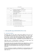


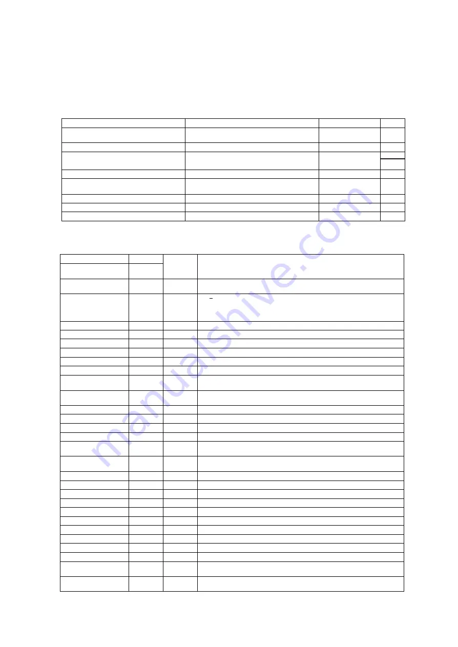
4.2.2
Operating Specifications
A
C
CHAR
A
CTER
I
ST
I
CS
TA
=
25•c,
Vee
=
1
2
V,
R
L
=
8 0
(u
n
less otherw
i
se
n
o
t
e
d
)
PARAM
E
TER
T
E
S
T
COND
I
T
I
ONS
M
I
N TYP MAX
U
N
I
T
Ks
v
R
S
u
pp
l
y
ripp
l
e
re
j
ec
t
i
o
n
200 m
V
pp
r
i
pp
l
e from 20
Hz-1k
H
z,
Ga
i
n
=
20
d
B,
I
n
pu
t
s ac
-
coupled
t
o AG
NO
-
7
0
dB
T
H
O
+
N
T
ota
l
ha
r
m
o
nic
d
i
s
t
ort
i
o
n
+no
i
s
e
R
L
=
8 0, f
=
1kH
z
,
P
o
=
3 W
(
h
a
lf
-
p
owe
r
)
0
.
06
%
Vn
Outpu
t
i
n
t
e
g
r
ated
n
o
i
s
e
20
H
z
to 22 k
Hz
,A
-
we
i
g
h
ted fi
lt
er, Ga
n
i
=
20 d
B
65
IJV
-80
d
B
V
Crossta
l
k
P
0
=
1
W
,
Ga
i
n
=
20 dB
,
f
=
1
kH
z
-
1
00
dB
SNR
Signa
-
l
t
o
-
nois
e r
a
t
o
i
M
a
x
i
mum o
u
tp
ut
a
t
THO
+
N
<
1%
,
f
=
1
k
Hz
,
Ga
i
n
=
20 dB, A
-
w
e
i
ghted
102
dB
fo
sc
Osci
ll
a
t
o
r
fr
e
qu
e
n
cy
2
50
3
1
0 350
k
H
z
T
herma
l
tr
i
p poi
n
t
1
50
·
c
T
h
e
rma
l
h
ysteresis
15
·c
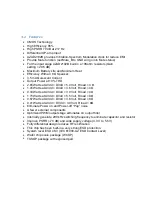
4.3
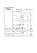
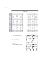
Pinning
P
I
N
110
/
P
D
E
S
C
R
I
P
T
I
ON
N
AM
E
P
i
n
Numbe
r
so
1
I
Sh
u
tdown
log
i
c
i
n
p
u
t fo
r
a
u
d
i
o a
m
p (
L
OW
=
ou
t
puts Hi
-
Z,
HIGH
=
ou
t
pu
t
s
enab
l
ed)
.
T
T
L
l
ogic
l
eve
l
s w
i
th comp
l
i
anc
e
to AVCC.
FAUL
T
2
0
Op
en
dra
i
n
ou
t
pu
t
used
to display short c
i
r
cuit o
r
de
de
t
ect fa
u
l
t
s
t
a
tu
s.
Vo
t
l
ag
e
comp
i
l
ant
t
o AVCC
.
S
h
o
rt
ci
r
cu
i
t fa
u
lts
can
be
set
t
o
a
u
to
-r
ecove
ry
by
co
n
necti
n
g
FAUL
T
p
i
n
t
o SO pi
n
. Otherwis
e
,
bo
th
s
h
ort c
i
r
c
u
i
t fa
u
l
ts and d
e
de
t
ect fa
u
lts
must
be reset
by
c
y
c
l
ing
PVCC
.
LI
NP
3
I
Pos
t
i
i
ve audio
in
p
u
t
f
or
l
eft c
h
a
n
neL
B
iased
at 3V.
LI
N
N
4
I
Nega
t
i
v
e
audio
i
npu
t
for
l
eft chan
n
e
L
Biased
at
3V
.
GAl
N
O
5
I
Ga
n
i
se
l
ec
t
leas
t
s
i
g
n
ifi
can
t
bit. TT
L
log
i
c
levels
w
i
th
c
om
p
l
ian
ce t
o
AVCC
.
GAI
N
1
6
I
Ga
n
i
s
e
e
l
ct
most s
i
g
n
i
f
i
can
t
b
i
t
TTL
l
ogic
l
eve
l
s w
i
th comp
l
ian
c
e
t
o AVCC.
AVCC
7
p
Ana
l
og s
u
pp
l
y
AGNO
8
A
n
a
l
og s
i
g
n
a
l
g
r
o
u
nd.
Connect to
the
t
h
e
r
ma
l
pa
d
.
GVOO
9
0
H
i
g
h
-
s
i
d
e
FET g
a
te dri
v
e su
p
p
l
y.
N
o
m
i
n
a
l
vo
l
tag
e
i
s
7V.
A
l
so should be
used
as supply
for P
LI
MIT fu
n
c
ti
o
n
P
LI
M
I
T
1
0
I
Power
l
i
m
t
i
level
ad
j
ust Co
n
nect a
r
es
i
sto
r
d
i
v
i
der from
GVOO
t
o
GND
to s
e
t
power
l
im
i
t.
Co
n
nec
t
d
i
rec
tl
y
t
o
GVOO
for
no power
l
i
mit.
R
I
NN
1
1
I
Nega
t
i
ve audio
i
npu
t
f
or
r
i
g
ht
c
h
a
n
ne
.
l
B
i
ased
at 3V.
R
I
NP
12
I
Posit
i
ve audio
in
p
u
t
f
or r
i
gh
t
channeL B
i
ase
d
a
t
3V.
NC
13
No
t
connected
PBTL
1
4
I
Pa
r
a
l
l
elB
T
L
mode
switc
h
PVCCR
1
5
p
Powe
r
supply for
r
i
gh
t
c
h
a
n
nel
H
-
b
r
i
d
g
e. R
i
ght c
h
a
n
n
e
l
and
left
c
h
a
n
n
e
l
powe
r
supply
i
nputs are co
n
nect
i
n
t
ernally
.
PVCCR
1
6
p
Power supply
f
or
r
i
g
h
t
channel
H
-
b
r
i
dge.
R
i
ght channel
and
l
eft
cha
n
n
e
l
power
supply
i
nputs are
co
n
nect
i
n
t
ernally.
BS
P
R
1
7
I
Bootstrap
11
0 fo
r
righ
t
chan
n
e
l
,
posit
i
ve h
i
gh-
s
i
d
e
F
ET.
O
U
TPR
1
8
0
C
l
ass
-
0
H
-
bridge pos
i
tive o
u
tp
u
t
f
o
r
r
i
g
h
t c
h
a
n
ne
l.
PGNO
1
9
Power
gro
u
nd for
t
he
H
-
br
i
dges
.
OU
T
NR
20
0
C
l
ass
-
0
H
-
bridge nega
ti
ve
outpu
t
f
or
r
i
g
h
t
c
h
a
n
ne
l.
BS
N
R
2
1
I
Bootstrap
1
/0 for right
chan
ne
l
,
negat
i
ve
h
i
g
h
-
s
i
d
e
FET.
BS
N
L
22
I
Bootstrap
1
/0 fo
r
left
c
h
a
n
ne
,
l
n
ega
t
i
ve high
-
side
F
ET
.
O
UT
NL
23
0
C
l
ass
-
0
H
-
bridg
e
n
e
gat
i
ve o
u
t
pu
t
for
l
e
ft
chan
n
e
l.
PGNO
2
4
Power
gro
u
nd for
the
H
-
b
r
i
dges
.
OU
T
PL
25
0
C
l
ass
-
0
H
-
bridge pos
i
tive o
u
t
put
f
or
l
eft
channe
L
BSPL
26
I
Bootstrap
1
/0 fo
r
left
c
h
a
n
ne
,
l
p
os
i
t
i
ve
h
igh
-
side F
E
T
.
PVCCL
27
p
Power supply
f
or
l
eft
channe
l
H
-
br
i
dge. Right channe
l
and
l
eft
channe
l
power
supply
i
np
u
ts
are
connec
t
i
n
t
ernally
.
PVCCL
28
p
Power supply
f
or
l
eft channe
l
H-
b
r
i
dge. Righ
t
chan
n
e
l
and
l
eft channe
l
p
ower
supply
i
nputs are connect
i
nternally.
Summary of Contents for VES1.1E
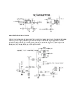
Page 21: ...5 1 Power management Power Management with Adaptor Power Management with PW25 PW26 ...
Page 22: ... Power Management with IPS16 IPS17 IPS60 PW05 Power Management with PW03 PW04 PW07 ...
Page 27: ...6 2 MSTAR block diagram ...
Page 40: ... Block Diagram of M88DS3002 14 3 Pin Assignment ...
Page 44: ......
Page 49: ...22 Connectors 22 1 SCART SC1 22 2 HDMI CN707 CN708 ...
Page 50: ... 22 3 VGA CN711 15 14 VERTICALSYNC 15 DOC CLOCK _ ...
Page 68: ......
Page 78: ...27 2 PSU ...
Page 79: ......


