


10-13
10-13
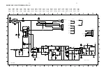
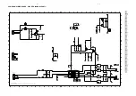
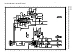
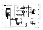
AVC BOARD - CIRCUIT DIAGRAM (PART 5)
RESET
POW SUPPL
COMP
BANDPASS
TEST
CTRL
SIGNAL
QUALITY
CLK
&
OSC
&
CLOCKED
(8th ORDER)
VSSA
DEM
RDS/RBDS
57 Khz
DET
V16
VDD
sink o.drain
V25
V26
V27
V28
-RESET
TEST
XTOUT
XTIN
-STOP
-INT0
-INT1
drain
P6-P9 source open drain
source open
drain 80k p.d.
80k pull down
P04
P05
P06
P07
80k pull down
80k pull down
80k pull down
V4
V5
V6
V7
V8
V9
V10
V11
V12
V13
V14
V15
CPU
VFT driver circuit (automatic display)
8-Bit A/D
Converter
8-Bit Input/Output
(tri-state)
P0
V17
V18
V19
V20
V21
V22
V29
V30
V31
V32
V33
V34
V35
V36
VKK
-SCK1
SI1
SO1
P03
PD
VSS
VAREF
VASS
XOUT
XIN
P5
TC2
-DV0
-SCKO
AIN0
AIN1
AIN2
AIN3
AIN4
P1
(tri state)
8-Bit Input/Output
P4
sink o.
3-B. I/O P3
AIN5
AIN6
AIN7
AIN10
AIN11
AIN12
AIN13
V0
V1
V2
V3
TC4
Counter
Program
ROM
RAM
8-Bit h. break. v.
(tri-state)
8-Bit Input/Output
SCA
SCL
INT4
INT2
TC1
V23
V24
output port with latch
output port with latch
out w. latch
P8
out. port w. latch
P
9
8-Bit h. breakdown v.
8-Bit high breakdown voltage
8-Bit high breakdown v.
5-Bit h. breakd. v.
out w. latch
( tristate )
8-Bit I/O P2
P7
P6
4-Bit In/Output
(tri-state)
*
*
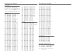
4530
820R
/22 version
@
@
@
@
With scart audio output muted in TV/AV mode
&
&
No muting in scart audio output
I
1530 A8
1531 A14
2530 H3
2531 H2
2532 I3
2533 I2
2550 D4
2551 C3
2552 C1
2553 D1
2554 C1
2560 G6
2562 I7
2563 H7
2564 H7
2565 H12
1
2
3
4
5
6
7
8
9
10
11
12
13
14
1
2
3
4
5
2K7
LX8000SA/37
None
6
7
8
9
10
11
12
13
14
A
B
C
D
E
F
G
H
I
A
B
C
D
E
F
G
H
*
2566 E12
2567 D6
2568 H8
2569 F11
2570 B11
2571 C12
2572 D4
2573 F8
2574 G9
2575 G9
2576 H9
2577 I8
2578 B11
2580 F2
2581 F3
3500 B10
3501 F9
GND_D
3502 B10
3503 B9
3504 D7
3505 D7
3506 D7
*
Version
*
3507 B9
3508 C7
3509 B8
3510 B8
3511 D7
3512 D6
3513 E7
3514 E7
3515 E7
3516 F8
3517 E8
3518 F8
3519 E8
3520 F8
3521 E9
3522 E10
3523 E10
3524 E10
3525 E10
3526 E10
3527 E10
3528 E10
3529 E11
3530 E11
Version
27K
%
3531 E11
3532 E11
3533 E11
3534 D11
3535 D11
3536 D11
3537 D11
3538 D11
3539 D12
3540 D11
3541 C12
3542 C11
3543 C12
3544 B11
3545 B11
3546 B10
3547 B10
3548 H8
For /22 version only
0 ohm
LX8000SA/21
12K
3549 G12
3550 D4
3551 D4
3552 C5
3553 D5
3554 E2
3555 E2
3556 C1
3559 A4
3560 H6
3561 H7
3562 I7
3563 H11
3564 H11
3565 H11
3566 I11
3567 G5
3568 H5
3569 A1
3570 E14
3568
#
#
*
## Not for /22 version
3571 D14
3572 A4
3573 A3
3574 B2
3575 A2
3576 B11
3577 B10
3579 B3
3580 B9
3581 B9
3582 B5
LX8000SA/22
LX7000SA/22
To Volume Rotary and IR_eye
3583 A5
3584 A6
3585 A7
3586 B9
3587 A3
3588 A6
3589 B2
3590 B5
3592 C7
3596 B10
3598 D13
3599 B8
4500 C6
4501 H7
4530 C6
5530 F9
%
Ghost key
*
Use 3K9 for LX8000SA/22
/ SAA6579
5531 F9
5532 F2
5533 B12
5581 H10
5582 C3
6531 B12
6532 B12
6533 F9
6534 G7
6535 G2
6536 B12
7531 C2
7532 H10
7533 H9
LX7000SA/21
LX8200SA/22
LPS
7534 H7
7535 A3
7536 B7
7537 A6
7538 B5
7539 B2
Key0, Key1 pull-up
1.19KHz
27K
3K9
*
No LPS
LPS OPTION
4500
MUTE_SCART
GND_D
470R
3507
3515
470R
GND_D
3546
470R
2551
GND_D
+D
GND_K
5
6
7
8
9
GND_D
1u
+5V6
3519
470R
3536 470R
+D
GND_D
GND_D
470R
100n
GND_D
100K
3561
3555
220K
470R
GND_D
+C
470R
3586
3509
470R
GND_D
GND_D
1u
2564
3501
3500
GND_D
10K
3564
2568
4n7
2562
GND_D
GND_D
1N4003
3
4
5
6
7
8
9
470R
3511
1530
FE-BT-VK-N
1
10
11
12
13
14
15
2
GND_D
1N4003
6536
2K7
3571
10K
3569
470R
3520
GND_D
4500
GND_D
4530
5533
2u2
3523
470R
2531
47u
+D
GND_D
3526
470R
470R
3502
6534
1N4148
GND_K
2532
100n
3574
10K
82p
2580
GND_D
47u
2571
GND_D
6531
1N4148
3518
470R
470R
3547
1K
3576
GND_D
+5V6
+5V6
10p
2573
470R
3524
GND_D
1n
2572
470R
GND_D
3533 470R
GND_D
3508
3510
GND_D
3584
390R
GND_K
3589
10K
470R
3528
GND_D
GND_D
100n
6533
BAS316
GND_D
+5V6
SCOUT
8
10
SYNC
15
TCON
VDDA
5
VDDD
12
3
VREF
6
VSSA VSSD
11
7531
SAA6581T
CIN
7
MODE
9
4
MPX
OSCI
13 14
OSCO
QUAL
1
RDCL
16
RDDA
2
1N4003
6532
GND_D
+D
+D
3513 470R
## 3553
10K
4501
3550
3522
470R
100n
10K
GND_D
2530
3542
BC847BW
7534
3543 470R
470R
3572
680R
+L
2560
10n
3566
1K
+5V6
3505 470R
470R
3580
3504 470R
4K7
3548
2K7
3567
GND_D
1K
3587
3K9
3568
+D
GND_K
22p
2575
22p
2569
GND_D
10K
3583
10K
3582
32K768
5531
DT-38
BC847BW
7539
2554
47p
3532
7538
BC847BW
3531 470R
470R
470R
+5V6
3503
GND_D
5581
2u2
3554
2K2
3559
10K
GND_D
3525
3538 470R
3521
GND_D
GND_D
+C
470R
6535
470R
3599
BC857BW
7537
3530
GND_D
GND_D
SDA
5
VCC
8
4
VSS
WC_
7
47R
M24C02
7532
E0
1
E1
2
E2
3
SCL
6
2577
1u
GND_D
470R
3544
470R
3527
470R
3577
470R
2578
5532
AT-51
4M332
1
2
3517
68
69
7
70
71
72
73
74
75
76
77
78
79
8
80
9
54
55
56
57
58
59
6
60
61
62
63
64
65
66
67
40
41
42
43
44
45
46
47
48
49
5
50
51
52
53
26
27
28
29
3
30
31
32
33
34
35
36
37
38
39
4
12 13 14 15 16 17 18 19
2
20 21 22 23 24
25
7536
TMP88CU74YF
1
10 11
470R
3516
10K
3556
3596
470R
GND_D
47u
2570
2566
100p
100p 2567
GND_D
10K
3579
3539
GND_D
3590
10K
GND_D
470R
2576
22p
2550
2u2
1M
3549
3598
10K
3565
1K
10K
47p
2581
3562
100K
GND_D
3563
470n
2563
3512 470R
22p
2574
47R
3529
GND_D
GND_D
3570
2K7
100n
2533
3514 470R
1K
3560
GND_D
470R
3537
+5V6
GND_D
GND_D
3541 470R
470R
+5V6_ECO
470R
3534
2553
560p
10K
## 3552
5582
2u2
5530
+D
470R
3581
GND_D
FE-BT-VK-N
1531
1
10
11
12
13
2
3
4
3545
470R
3592
470R
3540
470R
2552
560p
3575
10K
390R
3585
+5V6
3506 470R
10K
+D
GND_D
7535
BC857BW
GND_D
GND_D
+D
2565
3588
1K
GND_D
2p2
7533
GND_D
470R
BC847B
10K
3551
3535
+L
GND_D
GND_D
680R
3573
+5V6
MUTE_LO
+L
S_ON
MUTE_C
AMP_ON
MUTE_S
DIG_IN_CTRL
LCD_BackLit
LCD_BackLit_Dim
TU_CLK
MUTE_LR_SUB
TU_RDS_IN
LCD_BackLit
LCD_BackLit_Dim
RC5
KEY1
KEY0
VolA
VolB
LPS_WAKEUP
LED_GRN
DVD_5V
C_ON
TU_ENABLE
TU_RDS_IN
LPS_LED
SACD_LED
STBY
DVD_ON
LCD_RESET
LED_GRN
LPS_WAKEUP
+L
SACD_LED
LPS_LED
PWD_DN
RC5
KEY1
LPS_WAKEUP
I2C_DATA
VolB
VolA
Options
KEY0
I2C_CLK
TU_DATA
LCD_A0
LCD_RW
LCD_Back_ON
Tu_RDSCLK
Tu_RDSData
PWD_DN
DI_LOCK
I2C_CLKS
I2C_CLKC
Tu_RDSCLK
I2C_DATA
I2C_CLK
TU_STEREO
KEY0
KEY1
Tu_RDSData
HP_DET
LPC
Options
RESET
LCD_Back_ON
LCD_D0
LCD_D1
LCD_D2
LCD_D3
LCD_D4
LCD_D5
LCD_D6
LCD_D7
LCD_Back_ON
LCD_RW
LCD_E
LCD_A0
LCD_RESET
MPOscShift
I2C_DATA_DVD
NTC
LCD_E
LCD_D0
IntReq_DVD
LCD_D1
+C
RESET
+L
I2C_CLK_DVD
+C
DC voltage measured in DISC mode PLAY
*
Provision in layout only
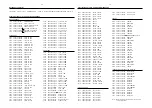
3139 118 56960...8239_210_91846...for 3518 pt1 dd wk0315
Note : Some values may varies, see respective
parts list for correct value.
AVC Circuit Diagram (Part 5)
3.4V
3.4V
0.7V
2.6V
0V
0.1V
2.4V
4.9V
2.5V
2.5V
2.5V
2.5V
0.1V
2.2V
4.9V
4.9V
0V
0.7V
3.4V
2.6V
0V
3.4V
"ON"
"ON"
0.2V
0.7V
4.9V
4.9V
4.9V


