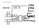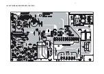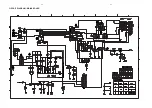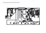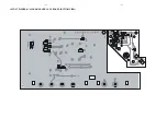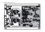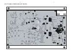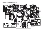
BRIEF INTRODUCTION OF THE AF9 BOARD
The AF9 Board consists of the following features :
a.
TDA7468D IC
TDA7468D IC (7501) which includes functions such as source selection, loudness control, dynamic bass control, treble
control, volume control and muting function. Sound features such as ALC, DBB, DSC and IS are controllable via I
2
C Bus
from the microprocessor.
The TDA7468D IC caters for 4 input sources namely TUNER, TAPE, CD and AUX. It also has a Mic mix input. In our
application, software will switch the input source to previous source MUTE during STANDBY mode and some other
occasions where noise from other input source is undesirable.
Note that the input to the TDA7468D IC must be ac coupled to prevent 'polp' noise.
Input networks are included to provide appropriate attenuation for various sources.
b.
SIMPLE MIC MIXING
The AF9 Board has provisions which can be configured to cater for one of the following:
MM : which caters for Mic mixing with additional Mic amplifier board.
NM : non Mic mixing.
c.
DOLBY PRO LOGIC (DPL) INTERFACE
The AF9 Board has provisions which can be configured to cater for DPL.
d.
LINE OUT
Line out cinch socket for connection to external amplifier.
e.
SUB-WOOFER OUT
Sub-woofer out cinch socket for connection to active sub-woofer speaker.
f.
INCREDIBLE SURROUND
Incredible surround effect using transistor circuit to create phase shifting and spatial effect.
g.
HEADPHONE AMPLIFIER
Headphone amplifier to drive 32 ohm to 1kohm headphone.
h.
CD STANDBY CONTROL
CD Standby Control circuit which switches on the supply to CD servo control IC, digital out buffer IC, HF circuit and the laser
light pen in CD mode only.
i.
ATTENUATION NETWORK
Attenuation network is provided at the output of the AF9 Board for interfacing with power board of different output power.
j.
CD DIGITAL OUT
CD Digital out cinch socket for connection to external digital audio decoders.
AF9 BOARD
TABLE OF CONTENTS
Brief Introduction of the AF9 Board ............................... 12-1
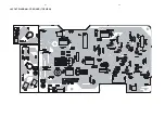
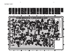
AF9 Board - Component layout ..................................... 12-2
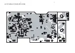
AF9 Board - Chip layout ................................................ 12-3
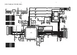
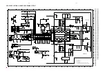
AF9 Board - Circuit Diagram (Part 1) ............................ 12-4
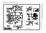
AF9 Board - Circuit Diagram (Part 2) ............................ 12-5
12-1
12-1
Summary of Contents for FWM583
Page 10: ...74HCT04D HEF4013BT 4 1 4 1 SET BLOCK DIAGRAM ...
Page 11: ...4 2 4 2 SET WIRING DIAGRAM ...
Page 12: ...5 1 5 1 PCB LAYOUT FRONT BOARD TOP VIEW ...
Page 13: ...5 2 5 2 PCB LAYOUT FRONT BOARD BOTTOM VIEW ...
Page 16: ...6 1 6 1 PCB LAYOUT MCU BOARD TOP VIEW ...
Page 17: ...6 2 6 2 PCB LAYOUT MCU BOARD BOTTOM VIEW ...
Page 20: ...9 1 9 1 LAYOUT DIAGRAM MAINS BOARD TOP VIEW ...
Page 25: ...8 2 8 2 LAYOUT DIAGRAM CD BOARD TOP VIEW ...
Page 26: ...8 3 8 3 LAYOUT DIAGRAM CD BOARD BOTTOM VIEW ...
Page 29: ...9 1 9 1 LAYOUT DIAGRAM MAINS BOARD TOP VIEW ...
Page 30: ...9 2 9 2 CIRCUIT DIAGRAM MAINS BOARD ...
Page 31: ...9 3 9 3 LAYOUT DIAGRAM MIC BOARD TOP VIEW LAYOUT DIAGRAM MIC BOARD BOTTOM VIEW ...
Page 33: ...10 1 10 1 LAYOUT DIAGRAM HIGH AMP USB JACK BOARD TOP VIEW ...
Page 34: ...10 2 10 2 LAYOUT DIAGRAM HIGH AMP USB JACK BOARD BOTTOM VIEW ...
Page 35: ...10 3 10 3 LAYOUT DIAGRAM POWER BOARD TOP VIEW ...
Page 36: ...10 4 10 4 LAYOUT DIAGRAM POWER BOARD BOTTOM VIEW ...
Page 37: ...CIRCUIT DIAGRAM HIGH AMP BOARD POWER BOARD 10 3 10 3 ...
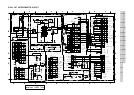
Page 41: ...12 4 12 4 SOURCE SELECTION SOUND PROCESSING CIRCUIT ...
Page 42: ...12 5 12 5 HEADPHONE AMPLIFIER I2 C EXPANDER CIRCUIT 1K ...

