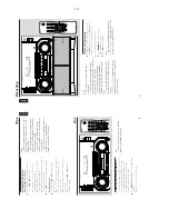


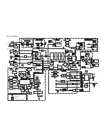


FRONT BOARD - CIRCUIT DIAGRAM
6-4
6-4
STB
D
1
EN1
SRG8
STB
D
1
EN1
SRG8
DEM
BAND
PASS
CTRL
CIRCUIT
AGC
INP
PIN
BIT
QUALITY
DIVIDER
AND
OSCILLATOR
FILTER
RECONSTRUCTION
(8th ORDER)
BANDPASS
ANTI-
ALIASING
FILTER
CLOCKED
COMPARATOR
REFERENCE
VOLTAGE
CLOCK
REGENERATION
AND SYNC
COSTAS LOOP
VARIABLE AND
FIXED DIVIDER
57 Khz
GENERATOR
DIFFERENTIAL
DECODER
BIPHASE
SYMBOL
DECODER
TEST LOGIC AND OUTPUT
SELECTOR SWITCH
VP1
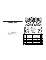
TMP87CS71F
7400
25 P00
26 P01
27 P02
28 P03
29 P04
30 P05
31 P06
32 P07
1
P10
2
P1
1
3
P12
4
P13
5
P14
6
P15
7
P16
8
P17
16
P20
10
P21
11
P22
17
P30
18
P31
19
P32
20
P33
21
P34
22
P35
23
P36
24
P37
67
P40
68
P41
69
P42
70
P43
71
P44
72
P45
73
P46
74
P47
75
P50
76
P51
77
P52
78
P53
79
P54
80
P55
34 P60
35 P61
36 P62
37 P63
38 P64
39 P65
40 P66
41
P67
42
P70
43
P71
44
P72
45
P73
46
P74
47
P75
48
P76
49
P77
50
P80
51
P81
52
P82
53
P83
54
P84
55
P85
56
P86
57
P87
58
P90
59
P91
60
P92
61
P93
62
P94
63
P95
64
P96
65
P97
12
RESET
9
TEST
33 VDD
66
VKK
15
VSS
13
XIN
14
XOUT
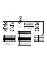
CLOCK/TIMING CONTROLLER
(I/O PORT 2)
C P U
I/O PORT 8
VDD
VKK
PROGR MEMORY
(ROM)
48KX8 BIT
8 BIT
TIMER/COUNTER
16 BIT
TIMER/COUNTER
INTERRUPT
CONTROLLER
6 BIT A/D-
CONVERTER
I/O PORT 7
I/O PORT 9
I/O PORT 1
I/O POR
T
0
I/O POR
T
6
I/O POR
T
4
I/O POR
T
5
I/O PORT 3
DATA MEMORY
(RAM)
1024X8 BIT
PROGRAM
COUNTER
3596
10K
D
3404
CDC1
Tape
K
L
M
A
B
C
D
E
F
G
H
I
J
K
L
M
1400 A9
1401 C1
1402 G1
1403 B2
1404 G16
1405 D13
1406 D14
1407 D14
1408 E13
CD
1
2
3
4
5
6
7
8
9
10
11
12
13
14
15
16
17
18
19
1
2
3
4
5
VCD_DSA_STR
CD_SILD
6
7
8
9
10
11
12
13
14
15
16
17
18
19
A
B
C
D
E
F
G
H
I
J
TU_STEREO
TpShClk
TU_GND
1409 I13
1410 E13
1411 E14
1412 E14
1413 E13
1414 E14
1415 E14
1416 F14
1417 E14
1418 F14
1419 F13
1420 F13
1421 G14
1422 F13
1423 F14
1424 G14
1425 H13
1426 F14
1427 H14
1428 G13
1429 G14
1430 G14
1431 G13
CDC2
F1
1432 G13
1433 H9
1434 J18
1435 K18
1437 G14
1438 G14
2400 A4
2402 B4
2403 B5
2404 A7
2405 A7
2406 B7
2407 B7
2408 D5
2409 D5
2410 F3
2411 F4
2412 F4
2413 F4
2414 F4
2415 F5
2416 F4
2417 G4
2418 A4
CDC3
CD_SHSTR
2419 I3
2420 H3
2421 I3
2422 H4
2423 J3
2424 K3
2425 K3
2426 K5
2427 L3
2428 K3
2429 L5
2430 L3
2431 L5
2432 B8
2433 B9
2434 A8
2435 C10
2436 D11
2437 D11
2438 A4
2439 G5
2440 G6
Tuner
GND_D
TpShStr
2441 G6
2442 G6
2443 G7
2444 G8
2445 G8
2446 H9
2447 G9
2448 G9
2449 I7
2450 I8
2451 I8
2452 H10
2453 H11
2454 J8
2455 J11
2456 D13
2457 D15
2458 A18
2459 B16
2460 D16
2461 D18
2462 E16
2463 H15
2464 J13
+5V6
TU_CLK
2465 K13
2466 K13
2467 K13
2468 M13
2469 K16
2470 K16
2471 J17
2472 J18
2473 L17
2474 L18
2475 F4
2476 A5
2477 A9
2478 A9
2479 J7
2480 A18
2481 D18
2482 D12
2483 D12
2484 J15
2485 G2
2486 L6
2487 B8
3400 A7
3401 A6
3402 B7
IS
F2
3403 B6
3404 B6
3405 C4
3406 C4
3407 D4
3408 G3
3409 G3
3410 G2
3411 G3
3412 G2
3413 G3
3414 G4
3415 H4
3416 B8
3418 I3
3419 K3
3420 K4
3421 K3
3422 K4
3423 L4
3424 L4
3425 L3
3426 L4
3427 L4
LOW_PWR_CTRL
SA_IN
3428 L4
3430 L6
3431 M6
3432 A6
3433 B6
3434 E6
3435 E6
3436 E6
3437 E6
3438 F6
3439 F6
3440 F6
3441 F6
3442 F6
3443 F5
3444 F6
3445 G6
3446 A9
3447 A8
3448 C8
3449 C9
3450 D6
3451 C6
3452 D6
3453 C6
3454 D7
3455 D7
3456 C7
TpShData
3457 D7
3458 C7
3459 D7
3460 C8
3461 D8
3462 C8
3463 D8
3464 C8
3465 D8
3466 C8
3467 D9
3468 C9
3469 D9
3470 C9
3471 D9
3472 C9
3473 D9
3474 C10
3475 D10
3476 C10
3477 D10
3478 C10
3479 D10
3480 D11
3481 D11
3482 E11
3483 E11
3484 E11
-Vkk
CD_SHDATA
+5V6
TU_ENABLE
3485 E11
3486 E11
3487 E11
3488 E11
3489 F11
3490 F11
3491 F11
3492 F11
3493 D4
3494 G7
3495 G7
3496 G7
3497 G7
3498 G7
3499 G8
3500 G8
3501 G8
3502 G8
3503 H9
3504 G9
3505 G9
3506 G9
3507 G10
MIC_DETECT
3508 G10
3509 G10
3510 J11
3511 J12
3512 B13
3513 B13
3514 B13
3515 B14
3516 C14
3517 B15
3518 B15
3519 C15
3520 D13
3521 E13
3522 E13
3523 E13
3524 G13
3525 F13
3526 F13
3527 G13
3528 G13
3529 H13
3530 H13
3531 I13
3532 I14
3533 I14
3534 I14
CD_SICL
8MHz
DBB
PW_DN
3535 K13
3536 K13
3537 M13
3538 M13
3539 M14
3540 M14
3541 E15
3542 E15
3543 F15
3544 A16
3545 A16
3546 B19
3547 B19
3548 B19
3549 E19
3550 F19
3551 E19
3552 D16
3553 D18
3554 D18
Aux
DSC
3555 C18
3556 C18
3558 F19
3559 G16
3560 H16
3561 H16
3562 H16
3563 I15
3564 J15
3565 K16
3566 K16
3567 J17
3568 J18
3569 K17
3570 K18
3571 H2
3572 G10
3573 G10
3574 G11
3575 G10
3576 I7
3577 I7
3578 H10
3579 H10
3580 I11
3581 I12
3582 C5
3583 E6
3584 K4
3585 J4
3586 I2
3587 B14
3588 B13
3589 B14
3590 B15
3591 E19
3592 E19
3593 F19
3594 G19
3595 F12
3596 A8
3597 C9
4400 C4
4401 C4
4402 D11
4403 H2
4405 M13
4406 M14
4414 C8
4415 C9
4416 H11
4417 G11
4522 D4
I2C_CLK
5400 B4
5401 A16
5402 C11
5403 I12
5404 L13
5405 G9
5406 G8
6400 A5
6401 A4
6402 A4
6403 B4
6404 B4
6405 B6
6406 L6
6409 E6
6410 E6
6411 M6
6412 C13
6413 C14
6414 C14
6415 C15
6416 D13
6417 E13
6418 E13
6419 E13
CLIPPING
GND_I2C
6420 F13
6421 F13
6422 F13
6423 G13
6424 G13
6425 H13
6426 H12
6427 B18
6428 B18
6429 B18
6430 E18
6431 F18
6432 E18
6433 D19
6434 D19
6435 C19
6436 C19
6437 F18
6438 E15
6439 E15
6440 E15
+5V6_CON
CD_GND
HP_DETECT
6441 J15
6447 F15
7400 G7
7401 I8
7402 K14
7403 M13
7404 A17
7405 D18
7406 B8
7407 B9
7408 H5
7410 I4
7411 L6
7413 C13
7414 C15
7415 K13
7416 J4
7417 K4
7418 L4
9400 C11
I2C_DATA
9401 C12
9402 H11
9403 C5
9404 I13
9405 H14
9406 H14
9407 E3
9408 E4
9409 E4
9410 D4
9411 E3
9481 G11
9488 F3
9505 J15
9508 I14
9509 I14
9540 B6
9541 A6
TpAdC1
TU_DATA
VEC
CD_SHCLK
CD_SWINFO
TpAdC2
+F
NTC
GND_D
2485
100p
4402
22p
# 2457
74HC4094D
7405
D
1K
3465
D
9402
3458
1K
D
1K
3462
3433
1R
3559
1K
TU
# 2438
100n
10K
3565
6432
FE-ST-VK-N
1403
1
2
3
4
3461
1K
D
560R
3549
3400
2R2
3479
1406
D
7402
TSOP2236
2454
2u2
D
1430
TU
1u
2423
1K
3495
47p
2452
9410
D
5
6
7
TU
3494
# 2460
100p
1
E0
2
E1
3
E2
6
SCL
5
M24C01
7403
3525
330R
2468
330R
TU
7418
BC857B
1u
2422
7410
BC847B
1N4148
6402
1u
2424
4K7
3542
1428
100p
3576
10K
3569
10K
2446
100u
2402
3459
1K
330R
3529
# 2462
100p
3440
1K
# 2408
10p
FTD
2475
47p
1405
10p
# 2409
6414
1K
3491
D
82K
3535
1437
3438
1K
9411
1424
1422
6418
2426
D
220n
# 3406
1K
2428
6n8
1K
3441
4401
9509
6430
D
270R
3463
1K
10n
6428
4u7
2405
D
TU
2404
4u7
6447
1N4148
10K
3418
1N4003
3442
1K
D
BC847B
7406
470p
# 2439
D
D
RES
2u2
5404
FTD
1K
3468
10K
# 3445
2425
1417
47n
100p
2487
3421
1K5
100n
2466
1407
XTAL
RDS
9404
D
22u
1419
3432
1R
2436
3484
1K
47n
2479
3471
1K
D
3572
1K
3567
10K
D
3509
1K
9508
47p
# 2421
TU
10K
351
1
1N4148
6438
D
6415
470p
# 2443
4M332
1433
AT
-51
1K
3498
3424
470K
100n
2465
1K
3474
10K
470K
47p
241
1
# 5402
2u2
3533
3577
# 2483
100n
3588
470R
6400
1N4148
1K5
330R
3524
D
1K5
3419
3506
1K
10K
3407
RES
3575
1M
560R
3558
IIC
100n
2476
3482
1K
3452
1K
3473
1K
D
2447
15p
3426
680K
1K
3444
1416
2414
47p
10K
3414
IIC
D
1K
3413
#
# 4414
# 3493
1429
3586
10K
150K
D
9401
3469
1K
1K
3481
4400
1K
3496
1K
3453
# 2420
47p
9481
D
1420
1K
3507
1K
3486
# 3480
1K
3510
10K
6429
1K
3456
2430
2472
10n
3532
470K
D
820p
470p
# 2442
11
9
10
1
16
8
D
3
2
15
4
5
6
7
14
13
12
D
BC857B
7417
2429
220n
3527
330R
D
1N4148
6417
3560
1K
1N4148
6419
47K
3431
3583
1K
1411
2u2
5401
3580
10K
6416
1N4148
D
D
3551
560R
D
100R
3449
3515
470R
7414
BC847B
# 2456
22p
100p
2433
BC847B
7408
3563
1K
3409
10K
100R
3439
6427
# 2441
470p
9
10
1
16
8
1409
TU
7404
74HC4094D
3
2
15
4
5
6
7
14
13
12
11
9408
3436
1K
1K
3412
1K
3437
6410
1N4148
D
6433
D
3483
1K
3K9
3539
D
2461
100n
D
6435
CD
D
100n
2410
9405
D
3574
1M
1K
100p
# 2459
1414
1K
3451
1415
3499
10K
220u
# 2464
7
8
9
6436
1
10
11
12
13
14
15
16
17
18
19
2
3
4
5
6
3
GND
1
OUT
VS 2
1401
FE-ST-VK-N
100n
2427
3513
470R
15p
2448
3401
220R
8
9
6401
1N4003
1402
FE-ST-VK-N
1
10
11
2
3
4
5
6
7
D
560R
3550
1413
IIC
FTD
100K
1K
3478
7415
3536
9488
BC847B
1K
3476
3477
1K
6437
D
1426
1N4148
6440
1K
# 3538
3555 270R
D
D
100n
2481
1N4148
47p
2412
3410
1K
SDA
8
VCC
4
VSS
7
WC_
3487
1K
1423
# 4415
330R
3526
# 2417
470K
3584
D
47p
10K
3568
1K
3470
3556 270R
3443
10K
1N4148
6409
2478
1412
CD
CST
5406
3546
270R
3523
330R
3579
2K2
7411
BC857B
1K
3490
47p
2415
L
TL-2R3VYKNT
L
TL-2R3VYKNT
6412
6434
3457
1K
D
12
3
MT1
4
MT2
5
3448
100R
1K
# 3540
1435
EC16
1K
3503
6431
4u7
2406
470R
3514
D
100p
2432
1N4148
3485
1K
2444
33p
6421
2n2
2470
2474
10n
3573
680K
1431
D
10K
3581
100p
# 2463
7416
BC857B
D
330R
3528
XTAL
6406
1N4148
D
EC16
1434
12
3
4
MT1
5
MT2
TU
3521
330R
47p
2416
1K
3435
FE-BT-VK-N
1404
1
2
3
4
3467
1K
T57
10
TEST
5 VDDA
12
VDDD
3 VREF
6
VSSA
11
VSSD
470K
3543
SAA6579T
7401
7 CIN
9
MODE
4 MUX
13
OSCI
14
OSCO
1
QUAL
16
RDCL
2
RDDA
8 SCOUT
15
1K
1K
3561
47p
3562
# 3582
1K
2453
3554
10n
2467
3423
10K
3505
1K
3411
D
6441
1N4148
3K9
3537
47p
# 2419
100R
3564
9403
# 3571
1K
1K
3472
6425
1N4148
#
#
#
#
680R
3518
330R
3545
3500
1K
3489
1K
3522
6439
1N4148
6403
4416
BC847B
7413
3455
1K
6413
330R
3520
100p
2435
3504
1K
3430
560R
2449
1n
2403
100n
1K
3566
2437
22u
3502
10K
2431
1K
3466
D
220n
2450
560p
1K
3497
1421
1K
3492
1K
3488
1N4003
1410
10K
3415
6404
100n
470K
3428
470R
3512
# 3405
10n
2473
1438
I2C
1K
680K
3422
1N4148
6424
4406
9407
10K
3408
D
D
# 2440
470p
10K
3508
2407
4u7
3427
82K
1K
3464
1K5
3425
1K
3454
32K768
5405
DT-38
D
D
2480
100n
2400
100u
10n
2471
1K
D
1427
1K
3460
D
BZX79-C5V6
6405
38
39
40
43
44
5
6
7
8
9
4405
17
18
19
2
20
27
28
29
30
31
32
33
34
35
36
37
1400
BJ794GNK
1
10
11
12
13
14
15
16
3578
220K
6422
1N4148
2413
47p
1425
CD
3420
82K
D
220R
3403
6420
1N4148
470R
3587
7407
BC847B
22K
82K
3446
D
1418
# 2482
100n
TU
4417
3541
4K7
3548
270R
680K
100p
2477
9409
3585
100n
2458
3450
1K
TU
2486
1u
3447
82K
10K
3434
3597
10K
3595
10K
D
1N4148
6426
5403
2u2
641
1
D
270R
3547
10K
3519
100n
# 2418
680R
3517
9406
9400
680R
3589
4u7
2484
3590
680R
100n
2455
# 9540
# 9541
3544
10K
D
3552
330R
2445
33p
3592
560R
3593
560R
3594
560R
# 2469
47n
3475
1K
D
1408
3516
10K
TU
I2C
IIC
# 4522
2R2
3402
4403
3591
560R
1K
3501
270R
3553
330R
1N4148
6423
2434
100p
3530
10K
3570
2u2
560p
2451
1432
D
5400
D
3534
3531
10K
9505
D
470K
+F
10K
3416
+5V6_CON
-FTD
Clipping
I2_CLK
KEY1
KEY2
+E
LowPwrWakeUp
KEY0
P02x
SA3
+LED
P05x
+F
+F
F2x
G09x
-FTD
-FTD
G09
G14x
-FTD
G10
-FTD
LowPwrWakeUp
NTC
F2
+5V6
-VKK
-FTD
P04x
+5V6
+LED
Standby
G14
LedShData
OSM
HPDet
+E
+5V6
P05
P05x
P03x
P03
OSM
P03x
MicDet
CdSwinfo
+5V6
+LED
+E
RdsClk
+5V6
+5V6
+F
TuEnable
P04x
SA1
SA3
CdShData
CdSiCl
-VKK
+5V6
+5V6_CON
CdSiLd
DSA_STR
F1
F2
+5V6_CON
+F
NTC
+F
I2_DA
T
F1
F1x
P01
LedShClk
LedShStr
+LED
LedShClk
BiPlaner
LedShStr
LedEnable
RC5
BiPlaner
+F
OPTIONS
CdShStr
CdShClk
SA_IN
PWDN
TuClk
+F
SA_IN
SA2
+F
+F
+5V6_CON
-VKK
+5V6
+F
TuCe
KEY1
KEY2
I2_DAT
G09
G1
1
G12
G13
G14
F1x
P01
P02
P03
P04
P05
P06
P07
P08
P09
P10
P1
1
P12
P13
P14
P15
P16
P07
+G
TuCe
JOGB
JOGA
+F
+F
VOLA
VOLB
P02
TuStereo
T
uEnable
G04
P04
I2_CLK
VOLA
G01
G02
G03
G05
G06
G07
G08
P08
P06
HPDet
P02x
MicDet
TuClk
+LED
+H
+H
SA1
Clipping
TpShData
TpShClk
KEY2
LedShClk
SA2
CdShData
I2_DA
T
CdShClk
RdsDat
JOGA
JOGB
KEY0
KEY1
OPTIONS
TpAdC1
TpAdC2
Reset
RdsClk
G03
RdsDat
TuDat
TuStereo
F2x
+F
TpShStr
+F
P11
P10
P04x
P09
TpShClk
G05
G06
G07
G08
G09x
G10
G1
1
G12
G13
G14x
P01
P02
P03
P04
P05
P06
P07
P08
P09
P10
P1
1
P12
P13
P14
P15
P16
CdShStr
G01
G02
G04
CdSiCl
CdSiLd
TpAdC2
TpAdC1
LedEnable
RC5
PWDN
CdSwinfo
Reset
VOLB
I2_CLK
T
uDat
DSA_STR
Standby
LedShData
LedShStr
TpShStr
TpShData
# : Provision.
: Refer to Variation Table.
Note : Some values may varies, see respective parts list for correct value.
3139 118 53880...88450 for...3442 pt1 dd wk0041
+G
( )
( )
[ ]
[ ]
[ ]
Summary of Contents for FW-C380
Page 61: ...10 3 Service Position ...
Page 62: ...10 4 Wiring ...
Page 75: ...10A 3 Service Position ...
Page 76: ...10A 4 Wiring ...


