


Circuit Descriptions and Abbreviation List
9.
1.
After closing switch 'S', the linear in time increasing current
I
T
, will charge capacitor C.
2.
Opening switch 'S' will generate a counter-e.m.f. in coil L,
trying to maintain current I
T
. This is possible via diode D
(this diode is also called 'freewheel diode'). Therefore, after
opening 'S', the magnetic energy stored in coil L will be
transferred to electrostatic energy in capacitor C. The V
IN
will only supply current during the time that 'S' is closed
while a constant current is flowing through R
L
.
3.
V
BAT
is directly proportional with V
IN
and the time that 'S' is
closed and reverse proportional with period time 'T'.
Therefore, by changing the duty cycle, it will be possible to
control V
BAT
.
Implementation
At start-up of the main supply, C2515 (diagram A1) can be
assumed as being a short-circuit. U
AB
will be 15 V (R3513,
D6510) and U
GS
of the FET will be +5.4 V (via D6515). The FET
will be driven into saturation (same as closing switch 'S'). The
drain-current will increase linear in time. With other words:
resistors R3513 and R3518 will start the oscillator.
The voltage across the co-coupled coil (4, 5) will keep the FET
into conductivity.
The TS7502 is a low-voltage semiconductor, which drives the
MOSFET TS7504. To bridge the different voltage levels, an
opto-coupler (item 7507) is used. Via this opto-coupler, the DC-
current through R3504 is influenced. The changed current
through R3504 changes the V
BE
of TS7502, which will
influence the drive of MOSFET TS7504 (= switch 'S' in figure
'Down-converter principle').
The sudden current interruption in the primary coil will induce a
counter-e.m.f. that wants to maintain the current via the
'freewheel' diode D6534. This current is linear decreasing in
time and, as it is also flowing through R3514//R3515, TS7502
will be blocked after a certain period. The gate of the FET will
be again made positive, is driven into conductivity and the cycle
starts again.
For safety reasons, transistor TS7530 is added as a back-up
solution for TS7502. If B-E of TS7502 is shorted, TS7530 takes
over its function.
Stabilisation of V
BAT
The output voltage V
BAT
is determined by: V
BAT
= V
IN
* (T
ON
/
(T
ON
+ T
OFF
)) = V
IN
* duty-cycle.
To stabilise the output voltage, a feedback loop is
implemented, which will reduce T
ON
when V
BAT
increases and
vice versa.
Via a voltage divider, existing of (1 %) resistors R3507, R3510,
and R3527//3549, a voltage of 2.5 V (when V
BAT
= 141 V) is fed
to the input of precision shunt regulator 7506. This regulator will
conduct, and a current will flow through the diode part of the
opto-coupler 7507. The base of TS7502 will now be set at a
certain positive voltage. As this transistor switches the FET
TS7504 'on' and 'off', this circuit can determine the duty-cycle.
E.g. when the load increases, V
BAT
will decrease.
Consequently, the input voltage of regulator 7506 will
decrease, resulting in a lower current. Via opto-coupler 7505
and transistor TS7502, T
ON
of the FET is changed (will
increase). The output voltage V
BAT
will rise.
If the load continues to increase, the regulator will block at a
certain moment. T
ON
is now at maximum value. This is the point
where V
BAT
will go below 141 V and, at further increasing load,
is switched 'off'. The voltage across the co-coupled coil (L5506,
pin 4 and 5) will decrease, due to the increasing load.
Therefore, the voltage on the gate of TS7504 comes below the
threshold voltage. The supply switches 'off', and an audible
hiccupping can be heard.
On the other hand when the load decreases, V
BAT
will rise.
Consequently, the input voltage of TS7506 will also rise,
resulting in a higher current. This changes the base voltage of
TS7502, and through that the T
ON
of the FET will decrease. The
output voltage V
BAT
will be reduced.
If, for instance, V
IN
will decrease (e.g. U
MAINS
is 180 V i.s.o. 240
V), the slope of the drain-current will be flattened, through
which the FET will be longer into conductance, keeping VOUT
constant.
If, for any reason, the stabilisation circuit might fail, the output
voltage V
BAT
can never exceed 200 V (via D6514). D6514 will
form a short-circuit, V
BAT
will drop and the set will switch 'off'
(this will also result in an audible hiccupping of the supply).
Switch to 'Standby' (via RC)
When the set is switched to 'Standby' mode via the Remote
Control, the Main supply is switched 'off' by the circuit around
TS7529 (see diagram A1).
During 'on'-state, the Main supply is fed with line pulses via the
'SUP-ENABLE' line. They are rectified and smoothed via
D6517, D6516, and C2530, and fed to TS7529. Because they
are less than -20 V, this transistor is blocked. When these
pulses are stopped, TS7529 will be saturated and TS7502 will
switch 'off'. This will switch 'off' the Main supply.
Set to 'On' (via 'SUP-ENABLE')
Via the 'STANDBY' command from the OTC, the MOSFETS
7141 and 7131 (diagram A2) are switched 'on'. When the +5V
and +8V are sensed by the OTC, a command is given to the
HOP to start the drive (via I
2
C).
When this is sensed via the 'SUP-ENABLE' line (at the base of
line transistor TS7421, diagram A3), the main supply is
switched 'on' via TS7529 (diagram A1).
Audio Supply
The pulses on the secondary winding of L5506 (or L5512) are
rectified by D6535 (+16 V) and D6536 (-16V), and smoothed by
C2542 and C2543.
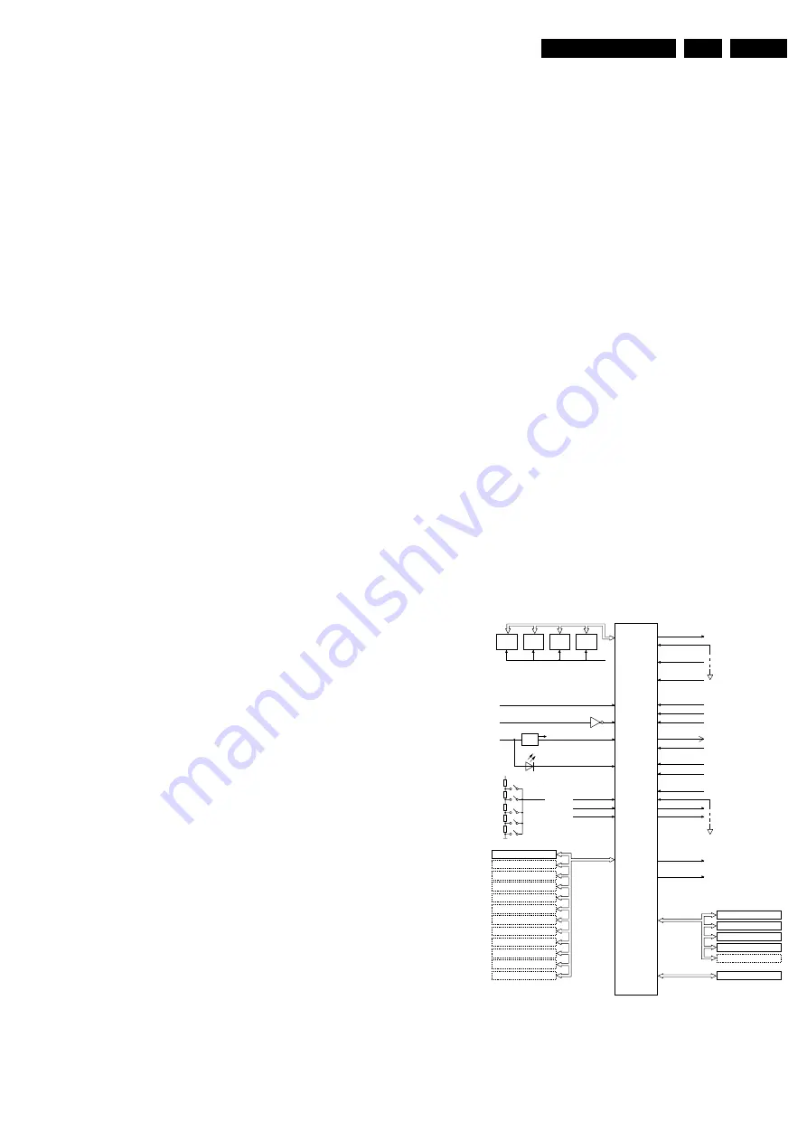
9.4
Control (Diagram B5)
Figure 9-9 Microprocessor (OTC)
CL 26532041_063.eps
110402
SAA5801
P50-OUT
SEL_IN_2
STATUS SC3
FRONT DETECT
120
A0...A19
D0...D15
CVBS-TXT
7001
5
KEYBOARD
107
+5V
106
+8V
105
+3V3
113
+5V2
RESET
ON/OFF-LED
74
H, V
83,84
119
117
109
LIGHT SENSOR
110
DEGAUSSING
115
108
SEL_IN_1
103
STANDBY
104
POR
99
RC5/RC6
100
P50-IN
97
SDM
4006
96
SOUND ENABLE
95
RESET AUDIO
94
RGB, BLENDING
77,78,79,80
87/88
91/92
FRAME
81
FLASH
EPG
FLASH
(SW)
DRAM
(TXT)
TUNER
SAM
4005
+3V3 +
RESET
+3V3
+3V3
I2C2
I2C1
85/86
slow
NVM
I2C3
fast
HIP
HOP
MSP
FBX
TOPIC
NVM
(PROG)
WIRELESS EXPANDER
WIRELESS TRANSMITTER
3D COMBFILTER
DVD ENGINE
MOIRÉ EXPANDER
AUTOSCAVEM DAC
DVD INTERFACE EXPANDER
PIP I/O EXPANDER
BOCMA PIP
SfH I/O EXPANDER
Vchip PIP
Summary of Contents for EM5E
Page 7: ...Directions for Use EN 7 EM5E 3 3 Directions for Use ...
Page 8: ...Directions for Use EN 8 EM5E 3 ...
Page 9: ...Directions for Use EN 9 EM5E 3 ...
Page 10: ...Directions for Use EN 10 EM5E 3 ...
Page 11: ...Directions for Use EN 11 EM5E 3 ...
Page 12: ...Directions for Use EN 12 EM5E 3 ...
Page 13: ...Directions for Use EN 13 EM5E 3 ...
Page 14: ...Directions for Use EN 14 EM5E 3 ...
Page 15: ...Directions for Use EN 15 EM5E 3 ...
Page 16: ...Directions for Use EN 16 EM5E 3 ...
Page 17: ...Directions for Use EN 17 EM5E 3 ...
Page 18: ...Directions for Use EN 18 EM5E 3 ...
Page 19: ...Directions for Use EN 19 EM5E 3 ...
Page 20: ...Directions for Use EN 20 EM5E 3 ...
Page 36: ...Service Modes Error Codes and Fault Finding EN 36 EM5E 5 Personal Notes ...