background image

EN 20

3139 785 32970

4.

Trouble Shooting

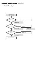
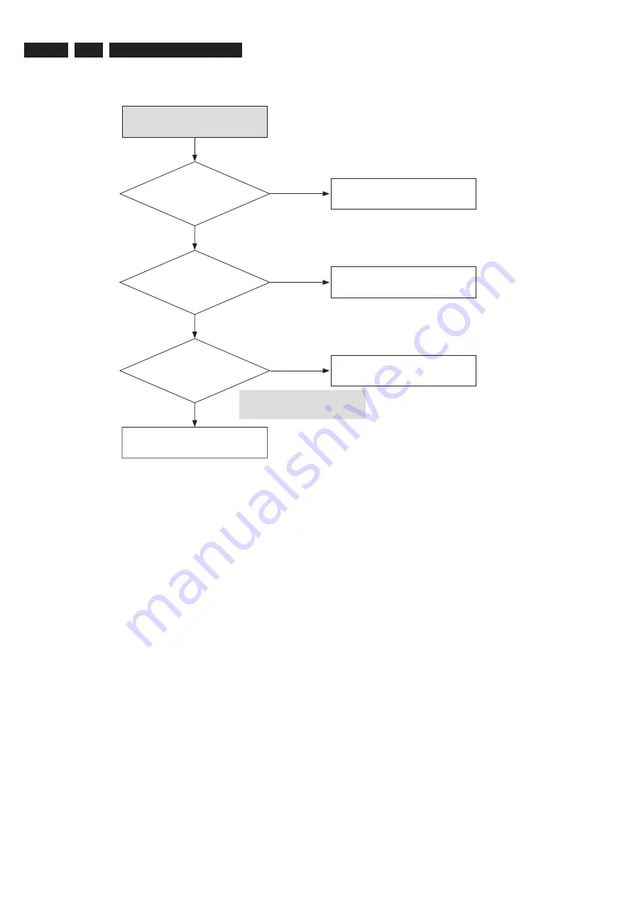
There is no Audio Output

Check

the Audio

signal at PIN 13,14,15,16

of AIC2

Check

the Audio

signal at pin1,2,37~48 of

AIC2

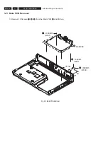
Check

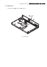
the Audio

signal at AIC4,5,6,7

Audio cable error

Replace the main PCB

Check AIC2 soldering or replace

AIC2

Check AIC4~7 soldering of

peripheral devices

No

Yes

No

No

Yes

Yes

Refer to Fig. 4-3

Summary of Contents for BDP7100/12

Page 1: ...uts 48 SMP8634 GPIO Control JTAG Debug Main PCB 48 MM1757 Analog Video Out Main PCB 49 PATA Control Main PCB 50 Power Main PCB 51 PCI ETC Main PCB 52 Front Interface Main PCB 53 Front Front PCB 54 Power Key Power Key PCB 55 7 PCB Layouts 56 Main PCB Component Side 1 56 Main PCB Component Side 2 57 Main PCB Conductor Side 2 58 S M P S PCB Component Side 59 S M P S PCB Conductor Side 60 Front PCB Co...

Page 2: ...d Chrominance 0 3Vpp 75Ω load HDMI 480p 720p 1080i 1080p 1 8 Video Performance 1 8 1 Component Video Outpuy Impedance 75 Ω SNR 60dB on all output Bandwidth Y 5 7MHz 3dB 480i 11 6MHz 3dB 480p 26 1MHz 1dB 720p 1080i Bandwidth PbPr 2 9MHz 3dB 480i 5 8MHz 3dB 480p 13MHz 1dB 720p 1080i Supports BD 1080i 720p 480p 480i DVD 480p 480i 1 8 2 Composite Video CVBS Output Impedance 75Ω SNR Luminance 65dB SNR ...

Page 3: ...EN 3 3139 785 32970 1 Location PCB Drawing MAIN PCB S M P S PCB BDP LOADER ASSY 1 11 PCB Location ...

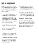
Page 4: ...ing system that complies with American National Standardsp institute ANSI C101 1 Leakage Current for Appliances and Underwriters Laboratories UL 1270 40 7 With the instrument s AC switch first in the ON position and then in the OFF position measure from a known earth ground metal water pipe conduit etc to all exposed metal parts of the instrument antennas handle brackets metal cabinets screwheads m...

Page 5: ...out of place or frayed wiring Do not change spacing between a component and the printed circuit board Check the AC power cord for damage 5 Components parts and or wiring that appear to have overheated or that are otherwise damaged should be replaced with components parts and or wiring that meet original specifications Additionally determine the cause of overheating and or damage and if necessary ta...

Page 6: ... precautions are indicated or printed on the cabinet chassis or components When servicing follow the printed or indicated service precautions and service materials 3 The components used in the unit have a specified flame resistance and dielectric strength When replacing components use components which have the same ratings Components identified by shading by or by in the circuit diagram are important...

Page 7: ...mbly 3 Use only a grounded tip soldering iron to solder or unsolder ESD devices 4 Use only an anti static solder removal devices Some solder removal devices not classified as anti static can generate electrical charges sufficient to damage ESD devices 5 Do not use freon propelled chemicals These can generate electrical charges sufficient to damage ESD devices 6 Do not remove a replacement ESD device ...

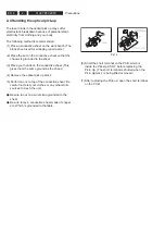
Page 8: ...your hands on the conductive sheet This gives them the same ground as the sheet 4 Remove the optical pick up block 5 Perform work on top of the conductive sheet Be careful not to let your clothes or any other static sources to touch the unit Be sure to put on a wrist strap grounded to the sheet Be sure to lay a conductive sheet made of copper etc Which is grounded to the table Fig 1 3 6 Short the ...

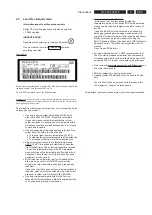
Page 9: ...ove 400 C otherwise wear out of tips will rise drastically and flux fluid will be destroyed To avoid wear out of tips switch off un used equipment or reduce heat Mix of lead free solder alloy parts with leaded solder alloy parts is poss ble but PHILIPS recommends strongly to avoid mixed solder alloy types leaded and lead free If one cannot avoid or does not know whether product is lead free clean ca...

Page 10: ...ssembly and Reassembly Cabinet and PCB CAUTION Connector Must be removed with care 3 1 Top Cabinet Removal 1 Remove 5 Screws 1 2 2 Lift up the Top Cabinet 3 in direction of arrow Fig 3 1 Top Cabinet Removal 3 SCREWS 3X10 B TOP CABINET 2 SCREWS 3X8 B 2 3 1 ...

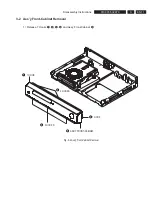
Page 11: ...5 32970 3 Disassembly Instructions 3 2 Ass y Front Cabinet Removal 1 Release 7 Hooks 1 2 3 4 and Ass y Front Cabinet 5 Fig 3 2 Ass y Front Cabinet Removal 1 HOOK ASS Y FRONT CABINET 2 HOOKS 3 HOOKS 1 HOOK 1 4 3 2 5 ...

Page 12: ...EN 12 3139 785 32970 3 Disassembly Instructions 3 3 Ass y Deck Removal 1 Remove 4 Screws 1 from the Ass y Deck 2 and lift it up Fig 3 3 Ass y Deck Removal 4 SCREWS 3X10 W ASS Y DECK 1 2 ...

Page 13: ...EN 13 3139 785 32970 3 Disassembly Instructions 3 4 S M P S PCB Removal 1 Remove 3 Screws 1 from the S M P S PCB 2 and lift it up Fig 3 4 S M P S PCB Removal 6 SCREWS 3X8 W S M P S PCB 1 2 ...

Page 14: ...139 785 32970 3 Disassembly Instructions 3 5 Main PCB Removal 1 Remove 10 Screws 1 2 3 from the Main PCB 4 and lift it up Fig 3 5 Main PCB Removal MAIN PCB 1 SCREW 3X6 B 4 SCREWS 3X6 W 5 SCREWS 3X10 B 1 4 2 3 ...

Page 15: ...EN 15 3139 785 32970 3 Disassembly Instructions 3 6 FAN Removal 1 Remove 2 Screws 1 from the Fan 2 and lift it up Fig 3 6 FAN Removal 2 SCREWS 5X14 S FAN 1 2 ...

Page 16: ...ower Detected Stand by LED OFF F1S01 is normal C1S01 voltage is normal voltage Switching operation of IC1S11 is normal Change the SMPS PCB Change fuse Change BD1 Change IC1S11 No Yes No No Yes Yes Refer to Fig 4 1 Refer to Fig 4 1 Refer to Fig 4 1 Refer to Fig 4 1 ...

Page 17: ...EN 17 3139 785 32970 4 Trouble Shooting Fig 4 1 Refer to S M P S PCB COMPONENT SIDE Refer to 1 Circuit Diagrams ...

Page 18: ...ng is PCM Set to Bitstream No Yes Check the A V Receiver can Decode Current Bit Steam No Yes Check Digital Audio Data at AIC 1 Pin 2 4 6 No Yes Check AIC1 soldering or replace AIC1 Digital Audio cable error Check the Audio Data at AIC1 Pin 13 No Yes Replace the Main PCB Refer to Fig 4 2 Refer to Fig 4 2 ...

Page 19: ...EN 19 3139 785 32970 4 Trouble Shooting Fig 4 2 DIGITAL AUDIO DATA AIC1 Pin2 4 6 13 Refer to Main PCB CONDUCTOR SIDE Refer to 9 Circuit Diagrams ...

Page 20: ...io signal at PIN 13 14 15 16 of AIC2 Check the Audio signal at pin1 2 37 48 of AIC2 Check the Audio signal at AIC4 5 6 7 Audio cable error Replace the main PCB Check AIC2 soldering or replace AIC2 Check AIC4 7 soldering of peripheral devices No Yes No No Yes Yes Refer to Fig 4 3 ...

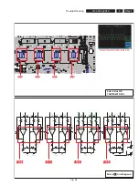
Page 21: ...EN 21 3139 785 32970 4 Trouble Shooting Fig 4 3 ANALOG AUDIO DATA AIC4 5 6 7 Refer to Main PCB COMPONENT SIDE 2 Refer to 9 Circuit Diagrams ...

Page 22: ...re Main and deck power OK 5v 12v Is the 40pin FFC cable between main deck inserted correctly Is the wave from of FCON1 PIN 25 normal MAIN PCB Change the deck Check the power Reinsert FFC cable correctly Change the Main board No Yes No No Yes Yes Refer to Fig 4 4 ...

Page 23: ...EN 23 3139 785 32970 4 Trouble Shooting Fig 4 4 FCON1 PIN 25 Refer to Main PCB COMPONENT SIDE 2 Refer to 12 Circuit Diagrams ...

Page 24: ...ork Remocon battery OK Is the FFC cable between Front panel Main OK FU3 PIN3 SIGNAL OK Check the Power of FMIC1 Pin51 or change the Main PCB Change the battery Re insert FFC cable correctly Check FU3 or change the Front panel PCB No Yes No No Yes Yes Refer to Fig 4 5 ...

Page 25: ...EN 25 3139 785 32970 4 Trouble Shooting Fig 4 5 Remote control eye data FU3 Pin3 Refer to Front PCB COMPONENT SIDE Refer to 16 Circuit Diagrams ...

Page 26: ... 26 3139 785 32970 4 Trouble Shooting No Picture Logo screen is OK NO LOGO HDMI No Yes HDMI No Yes BD DVD Playback is OK No Yes CHANGE THE MAIN PCB NO LOGO Component Component No Yes NO LOGO CVBS S Video ...

Page 27: ...1 is High 2 0 5 0V HDMI cable error Check the Video select cable connection TV mode Check MIC1 power input UX7 oscillation Memory interface Check HCN1 Connector and HDMI cable connection No Yes No No Yes Yes data output from HIC6 pin30 31 33 34 36 37 39 40 Check the HIC1 power input and peripheral devices No Yes Refer to Fig 4 6 Refer to Fig 4 7 Refer to Fig 4 6 ...

Page 28: ...EN 28 3139 785 32970 4 Trouble Shooting Digital Video signal MIC1 HRN1 HRN6 UX7 CLOCK SIGNAL 27MHz Fig 4 6 Refer to Main PCB COMPONENT SIDE 2 Refer to 6 Circuit Diagrams Refer to 10 Circuit Diagrams ...

Page 29: ...EN 29 3139 785 32970 4 Trouble Shooting Fig 4 7 HDMI OUTPUT DATA HIC6 pin30 31 33 34 36 37 39 40 Refer to 6 Circuit Diagrams Refer to Main PCB COMPONENT SIDE 2 ...

Page 30: ...cable connection and TV mode Video output from MIC1 VE26 27 28 Video output from VIC3 VR37 VR44 VR46 Component cable error Check the Video select cable connection TV mode MIC1 soldering error Check VIC3 soldering of peripheral devices No Yes No No Yes Yes Refer to Fig 4 8 Refer to Fig 4 9 ...

Page 31: ...EN 31 3139 785 32970 4 Trouble Shooting Fig 4 8 Pr Color bar Pin MIC1 VE28 Pb Color bar Pin MIC1 VE27 Y Color bar Pin MIC1 VE26 Refer to Main PCB COMPONENT SIDE 2 Refer to 11 Circuit Diagrams ...

Page 32: ...EN 32 3139 785 32970 4 Trouble Shooting Fig 4 9 Y Color bar Pin VR37 Pr Color bar Pin VR46 Pb Color bar Pin VR44 Refer to Main PCB CONDUCTOR SIDE Refer to 11 Circuit Diagrams ...

Page 33: ...cable connection and TV mode Video output from MIC1 VC2 VC3 VC4 Video output from VIC1 VR7 VR21 VR22 Component cable error Check the Video select cable connection TV mode MIC1 soldering error Check VIC1 soldering of peripheral devices No Yes No No Yes Yes Refer to Fig 4 10 Refer to Fig 4 10 ...

Page 34: ...39 785 32970 4 Trouble Shooting Fig 4 10 Y Color bar Pin MIC1 VC2 VIC1 VR7 C Color bar Pin MIC1 VC3 VIC1 VR21 CVBS Color bar Pin MIC1 VC4 VIC1 VR22 Refer to Main PCB CONDUCTOR SIDE Refer to 11 Circuit Diagrams ...

Page 35: ...sc the set will display OPEN And on the TV screen it will show Firmware Update Do you want to update Firmware Please remove a disc from the tray Current Version 070913 02_12 New Version 070925 01_12 4 Remove the upgrade disc and select Yes to continue While updating the firmware on the TV screen it will show Firmware Update Now Processing Please do not turn off the power And the set will display CD...

Page 36: ...kip forward key on the Front Panel of the set as shown in figure 1 Figure 1 3 The initial mode will be activated and the set will display NO DISC 4 On the TV Screen it will show the language selection menu as shown in figure 2 and select the Language by pressing the corresponding key as described in the menu Figure 2 Note Resetting the initial mode will restore all the user settings to Default ...

Page 37: ...EN 37 3139 785 32970 6 Block and Wiring Diagram 6 1 All block Diagram ...

Page 38: ...EN 38 3139 785 32970 6 Block and Wiring Diagram 6 2 Wiring Diagram ...

Page 39: ...EN 39 3139 785 32970 7 Circuit Diagrams and PCB Layouts S M P S S M P S PCB 7 Circuit Diagrams and PCB Layouts Circuit Diagrams 1 ...

Page 40: ...EN 40 3139 785 32970 7 Circuit Diagrams and PCB Layouts SMP8634 DDR SDRAM Main PCB Schematic Diagrams 2 ...

Page 41: ...EN 41 3139 785 32970 7 Circuit Diagrams and PCB Layouts SMP8634 Flash Memory Main PCB Schematic Diagrams 3 ...

Page 42: ...EN 42 3139 785 32970 7 Circuit Diagrams and PCB Layouts Schematic Diagrams Nand Flash Controller Main PCB 4 ...

Page 43: ...EN 43 3139 785 32970 7 Circuit Diagrams and PCB Layouts SMP8634 Power Decoupling Main PCB Schematic Diagrams 5 ...

Page 44: ...B Layouts Sil9134 HDMI Main PCB Schematic Diagrams HDMI OUTPUT DATA HIC6 pin30 31 33 34 36 37 39 40 These are the waveforms of BD P1400 Caution There can be some differences Voltage Frequency stc among cameras Digital Video signal MIC1 HRN1 HRN6 6 ...

Page 45: ...EN 45 3139 785 32970 7 Circuit Diagrams and PCB Layouts HDMI CEC Main PCB Schematic Diagrams 7 ...

Page 46: ...EN 46 3139 785 32970 7 Circuit Diagrams and PCB Layouts Ethernet contol Main PCB Schematic Diagrams 8 ...

Page 47: ...agrams and PCB Layouts Audio Main PCB Schematic Diagrams DIGITAL AUDIO DATA AIC1 Pin2 4 6 13 These are the waveforms of BD P1400 Caution There can be some differ ences Voltage Frequency stc among cameras ANALOG AUDIO DATA AIC4 5 6 7 9 ...

Page 48: ...rcuit Diagrams and PCB Layouts SMP8634 GPIO Control JTAG Debug Main PCB Schematic Diagrams UX7 CLOCK SIGNAL 27MHz These are the waveforms of BD P1400 Caution There can be some differ ences Voltage Frequency stc among cameras 10 ...

Page 49: ... Color bar Pin MIC1 VE28 VR46 Pb Color bar Pin MIC1 VE27 VR44 Y Color bar Pin MIC1 VE26 VR37 Y Color bar Pin MIC1 VC2 VIC1 VR7 C Color bar Pin MIC1 VC3 VIC1 VR21 CVBS Color bar Pin MIC1 VC4 VIC1 VR22 These are the waveforms of BD P1400 Caution There can be some differences Voltage Frequency stc among cameras 11 ...

Page 50: ... 785 32970 7 Circuit Diagrams and PCB Layouts PATA Control Main PCB Schematic Diagrams FCON1 PIN 25 These are the waveforms of BD P1400 Caution There can be some differences Voltage Frequency stc among cameras 12 ...

Page 51: ...EN 51 3139 785 32970 7 Circuit Diagrams and PCB Layouts Power Main PCB Schematic Diagrams 13 ...

Page 52: ...EN 52 3139 785 32970 7 Circuit Diagrams and PCB Layouts PCI ETC Main PCB Schematic Diagrams 14 ...

Page 53: ...EN 53 3139 785 32970 7 Circuit Diagrams and PCB Layouts Front Interface Main PCB Schematic Diagrams Power 15 ...

Page 54: ... 7 Circuit Diagrams and PCB Layouts Front Front PCB Schematic Diagrams Power Remote control eye data FU3 Pin3 These are the waveforms of BD P1400 Caution There can be some differences Voltage Frequency stc among cameras 16 ...

Page 55: ...EN 55 3139 785 32970 7 Circuit Diagrams and PCB Layouts Power Key Power Key PCB Schematic Diagrams 17 ...

Page 56: ...LOC NO X Y UCON1 A 0 CEIC1 A 0 CEC CON1 A 2 PIC4 A 3 PIC3 A 4 PIC7 A 5 MIC6 B 1 MIC9 B 2 UIC7 B 3 AIC2 B 4 AIC6 B 5 MIC2 C 0 AIC5 C 5 AIC4 C 5 MIC4 D 0 MIC1 D 2 PIC1 E 1 FPCON1 F 0 NIC1 F 2 PCI1 F 3 HIC6 F 4 FCON1 H 0 PCB Layout Diagrams 1 COMPONENT SIDE Layout Main PCB ...

Page 57: ...ams FCON1 PIN 25 Pr Color bar Pin MIC1 VE26 Pb Color bar Pin MIC1 VE27 Y Color bar Pin MIC1 VE28 Digital Video signal MIC1 HRN1 HRN6 UX7 CLOCK SIGNAL 27MHz HDMI OUTPUT DATA HIC6 pin30 31 33 34 36 37 39 40 ANALOG AUDIO DATA AIC4 5 6 7 Layout Main PCB 2 COMPONENT SIDE ...

Page 58: ...in MIC1 VC2 VIC1 VR7 C Color bar Pin MIC1 VC3 VIC1 VR21 CVBS Color bar Pin MIC1 VC4 VIC1 VR22 LOC NO X Y AIC1 A 5 U2505 B 1 U2504 B 2 U7 B 2 HIC7 B 3 HIC10 B 4 PIC77 C 1 MIC3 D 0 VIC3 D 4 MIC5 E 0 VIC1 E 4 PIC11 G 0 PIC5 G 3 CONDUCTOR SIDE Pr Color bar Pin VR46 Pb Color bar Pin VR44 Y Color bar Pin VR37 Layout Main PCB ...

Page 59: ...EN 59 3139 785 32970 7 Circuit Diagrams and PCB Layouts Layout S M P S PCB PCB Diagrams COMPONENT SIDE LOC NO X Y CN2 A 0 CN1 A 1 IC2S51 C 3 IC1S81 E 1 IC1S12 E 1 IC1S11 F 1 ...

Page 60: ...EN 60 3139 785 32970 7 Circuit Diagrams and PCB Layouts PCB Diagrams CONDUCTOR SIDE Layout S M P S PCB ...

Page 61: ...EN 61 3139 785 32970 7 Circuit Diagrams and PCB Layouts Layout Front PCB PCB Diagrams COMPONENT SIDE CONDUCTOR SIDE Remote control eye data FU3 Pin3 ...

Page 62: ...EN 62 3139 785 32970 7 Circuit Diagrams and PCB Layouts Layout Power Key PCB PCB Diagrams COMPONENT SIDE CONDUCTOR SIDE ...

Page 63: ...EN 63 3139 785 32970 8 Exploded view and Service Parts List P025 W001 M210 W348 W271 W344 W009 W001 W009 P001 P003 H003 P030 P006 P005 C001 A001 C015 W348 PCBAL PCBAR 8 Cabinet Assembly ...

Page 64: ...E CONNECTOR 15 PIN F1S01 996510008968 FUSE 2A 250V SLOW BLOW FFC1 996510008909 FLEX CABLE 23PIN FRONT TO MAIN FFC2 996510008910 FLEX CABLE 40P LOADER TO MAIN H003 996510008908 BDP LOADER ASSY M210 996510008898 WASHER HEX SCREW P001 996510008902 MAIN PCBA ASSY P003 996510008967 SMPS PCBA ASSY P025 996510008896 POWER CORD W CONNECTOR P030 996500042116 FAN DC 12V 20mA 2000rpm 0 125m W271 996520032549...

Page 65: ... the audio cable into the TV 4 5 6 TV Note This type of audio video connection does not support Blu ray disc playback Option 2 Using HDMI best quality 1 2 3 HDTV A Take a HDMI cable not supplied B Plug one end of the HDMI cable into the HDMI OUT socket C Plug the other end of the HDMI cable into the HD compliant TV Note This type of connection requires no audio connection B Connect to the power ou...

Page 66: ...4 für Deutsch Premere 5 per Italiano Druk op 6 voor Nederlands Prima 7 para Português MENU LANGUAGE SELECTION Read the instructions on the TV and use the BDP7100 remote control to select your preferred language Wait a few seconds for the player to fi nish initialising the system The BDP7100 is now ready for use STOP Need help User Manual See the user manual that came with your Philips product or d...

Page 67: ...EN 67 3139 785 32971 10 Revision List 10 Revision List Version 1 0 Initial Release Version 1 1 Changes in Service Parts ...

Reviews: