


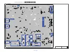


Circuit Diagrams and PWB Layouts
10.
10-6-9
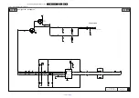
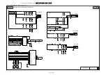
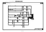
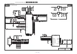
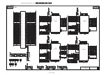
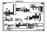
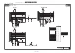
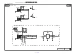
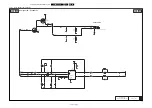
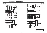
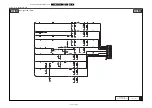
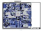
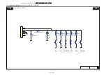
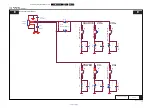
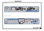
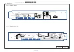
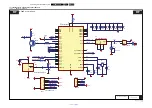
B05B, Digital I/O - USB
19510_52
3
_1
3
0412.ep
s
1
3
0412
Digit
a
l I/O - U
S
B
B05B
B05B
201
3
-01-11
1
3
1
3
9 12
3
6545
PCB
S
B
SS
B
MT5
3
96 R
3
LATAM 2K1
3
+T
VIN
VOUT
GND
EN
FLG
EN
+T
+T
+T
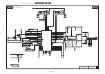
U
S
B PORT 1
For integr
a
ted WiFi
S
Q Te
s
t Only
0R
0R
(WiFi)
45R
3
INTERNAL U
S
B
0R
45R
3
U
S
B PORT 2
+5V_U
S
B2
0R
FC62
FC
3
7
FC61
1
FC11
4
3
2
5
FC42
RE
S
RT9715GGB
7C01
FC21
+
3
V
3
_
S
W
FC
3
9
3
C06
0R
3
100K
+
3
V
3S
TBY
5
RE
S
3
C05
3
C04-4
RE
S
4
3
C04-1
1
8
RE
S
FC
3
6
FC4
3
4
5
6
2C19
100n
U
S
B-16-PBT-B-
3
0-CU1-BRF
1
2
3
FC
38
1C0
3
3
C21
0R
3
3
C04-2
27
RE
S
0R
3
3
C
3
1
2C01
100n
RE
S
FC
3
2
+5V_
S
W
RE
S3
C04-
3
3
6
RE
S
2C02
10
u
FC46
FC51
1
2
3
4
5
6
+5V_U
S
B2
+5V_U
S
B
3
1C02
U
S
B-16-PBT-B-
3
0-CU1-BRF
RE
S
1
%
3
C
33
1
u
0
2C0
3
0R
3
3
C11
RE
S
3
100n
2C17
1C
3
2
ACM2012
1
4
2
+5V_
S
W
FC45
FC44
U
S
B_PWR_P0
2C1
8
100
u
6.
3
V
3
4
5
6
7
8
+
3
V
3
_WOLAN
1C
3
1
S
1
3
15
1
2
+5V_
S
W
+5V_U
S
B
3
3
C
3
2
RE
S
+
3
V
3
_WOLAN
1
%
U
S
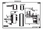
B_DP_WIFI
6.
3
V
100
u
2C20
IRQ_WOWLANn
U
S
B_DM_WIFI
ENABLE_WOWLAN
U
S
B_DP2
U
S
B_DM2
U
S
B_DP1
U
S
B_DM1


