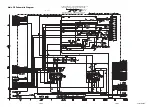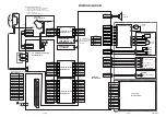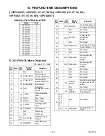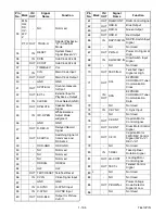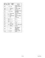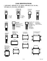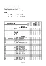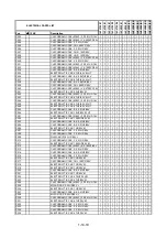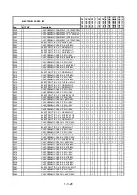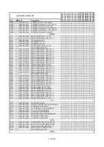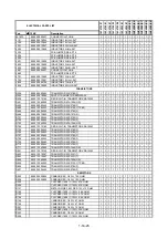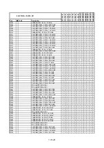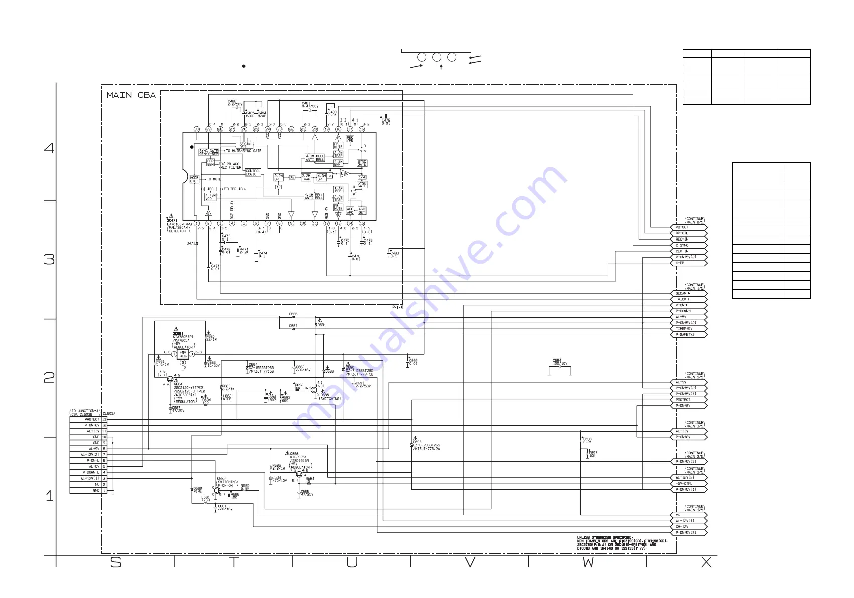
Main 4/5 Schematic Diagram
1-8-52
1-8-53
T6410SCM4
“ “ = SMD
Voltage indications for PLAY and REC modes on
the Schematic Diagrams are as shown below:
1
2
3
5.0
(2.5)
~
5.0
THE SAME VOLTAGE FOR
BOTH PLAY & REC MODES.
INDICATES THAT THE VOLTAGE
IS NOT CONSISTENT HERE.
PLAY MODE
REC MODE
“ “ = SMD
VOLTAGE CHART (Power off mode)
Ref. No.
IC602
Ref. No.
Q682
Q684
Q685
Q686
0
3.1
0
0.1
3.1
0
0
0.6
0
1
2
3
3.2
0
1.9
0
7.9
0
E
C
B
Comparison Chart of
Models and Marks
MODEL
MARK
14PV225/07
M
14PV225/01
N
14PV225/58
O
14PV225/39
P
14PV422/07
Q
14PV422/01
R
14PV422/58
S
14PV422/39
T
14PV125/07
U
14PV125/01
V
14PV125/58
W
14PV125/39
X
14PV120/07
Y
14PV425/07
Z


