background image

16

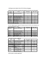
V-out

Field driving pulse output;

17

H-Vcc

Connect   to   8V   power   supply   of   DEF   (deflection 
circuit);

18

TV GND

Analog circuit grounding pin;

19

Cb

Cb component signal input terminal;

20

E/W-OUT

E/W signal output terminal;

21

Cr

Cr component signal input terminal;

22

EXT-AU1

AUDEO1 input;

23

C-in

Color intensity signal input terminal;

24

V2

Video signal CVBS/Y input terminal;

25

ACL

ACL filter interface;

26

TV-in

TV video signal input terminal;

27

ABC-in

ABCL   (color   saturation,   brightness   limit)   signal 
input;

28

Audio-out1

Audio signal output terminal 1, with volume control 
function;

29

Audio-out2

Audio signal output terminal 2, with volume control 
function;

30

TV-out

PIF detector signal (full TV signal) output;

31

SIF

Sound intermediate frequency output (can have no 
connection of peripheral circuit);

32

EXT-AU2

AUDEO2 input;

33

SIF in

Input sound second intermediate frequency signal 
or horizontal phase correction signal;

34

DC NF

Connect to capacitor;

35

PIF•PLL

Connect to PIF-PLL loop filter;

36

IF-5V

Connect   to   intermediate   frequency   circuit   block 
power of 5V;

37

S-Reg

Connect to filter capacitor to stabilize internal bias;

38

AU OUT

Audio output without volume control;

39

IF AGC

Connect to IF AGC filter;

40

IF GND

Intermediate frequency grounding terminal;

41

IF in

Pin41   and   Pin42   are   two   input   terminals   of   the 
differential   amplifier;   input   the   intermediate 
frequency signal from acoustic surface wave filter.

42

IF in

43

RF AGC

Output RF-AGC control voltage to high frequency 
tuner;

44

Black Det

Connect to black level detection filter;

45

Monitor out

Output CVBS/SVM signal from this terminal, CVBS/
SVM signal is selected through I²C bus.

46

APC fil

Connect   to   the  APC   filter   of   the   color   decoding 
circuit;

47

YC VCC5V1

YC power input;

48

SYNC OUT

Compound synchronous signal output;

49

DVCC—3.3V

Digital circuit power supply pin;

50

R out

Output baseband R signal to video amplifier circuit;

51

G out

Output baseband G signal to video amplifier circuit;

52

B out

Output baseband B signal to video amplifier circuit;

53

GND

Connect to analog grounding line.

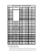
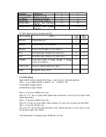
V. Remote Control Part (Key Value Table)

Summary of Contents for TU2191

Page 1: ...TU2191 Frequency Synthesis Color TV Maintenance Manual ...

Page 2: ...ions II Main Technical Specifications III System Constitution Block Diagram IV Pin Assignment Table and IC Pin Function Description V Remote Control Part Key Value Table VI Circuit Principle Analysis VII Main IC Introduction VIII Notes for Factory Debugging ...

Page 3: ...turn function 7 Image mode personal dynamic standard gentle and single key selection 8 Image parameter adjustment brightness contrast color intensity definition tone 9 Mute control mute when mute ON OFF program switching and AV switching 10 Scheduled power on off and program reservation 11 Automatic shutdown when no signal at TV state for 15 minutes 12 Unique semi transparent menu display 13 Engli...

Page 4: ...rior notice For details confirm with the real product X RAY RADIATION WARNING 1 The possible X ray radiation source I the device is the high voltage part and the kinescope 2 In order to guarantee the TV set does not generate X ray radiation make sure the kinescope high voltage ignition coil and line operate in normal condition without aging Note In order to prevent X ray radiation designated kines...

Page 5: ...W Cb Cr CRT IV TMPA8873 XXXX Pin Assignment Table SAWF KEY MATRIX RECEIVEERMP TC4053 AV SW FBT T471 LA78040 TDA9302 LA78041 TDA8177 TA9028 023 022 LA7461 SC6122 EEPROM 8K bit 2 in Chip TMPA8873 XXXX TA1304 TA1343 BTSC AN5832 or LA72700 4053 Vout Hout SIF ...

Page 6: ...TMPA8899 XXXX Pin and Function Description ...

Page 7: ...61 MUTE Mute level control mute output high level 62 NO USE 63 RMT IN Remote signal input 64 Power Power control initial low level valid controlled by F11 ontime item Notes for terminal control output state 0 stands for low level 1 stands for high level Pin3 indication Value range for keys central value in the range of key voltage is recommended KEY Off P P V V MENU TV AV POWER Value range Sanyo 0...

Page 8: ...een AV mutes without signal 1 When there is no blue screen AV does not mute without signal 2 Signal processing part 11 TV GND Analog circuit grounding pin 12 FBP IN FBP fly back pulse input terminal 13 H out Horizontal driving pulse output terminal 14 H AFC Horizontal AFC circuit connection terminal for external filter voltage of the terminal controls H VCO frequency 15 V SAW Connect to external s...

Page 9: ... 35 PIF PLL Connect to PIF PLL loop filter 36 IF 5V Connect to intermediate frequency circuit block power of 5V 37 S Reg Connect to filter capacitor to stabilize internal bias 38 AU OUT Audio output without volume control 39 IF AGC Connect to IF AGC filter 40 IF GND Intermediate frequency grounding terminal 41 IF in Pin41 and Pin42 are two input terminals of the differential amplifier input the in...

Page 10: ...01 11 11 0x13 0x1b K19 Vol Volume minus key 00010010 12 12 0x14 0x1e K20 Vol Volume plus key 00010011 13 13 0x10 0x1f K21 MUTE Mute key 00010100 14 14 0x16 0x15 K22 SLEEP Sleep key 00010101 15 15 0x0f 0x19 K23 DISP LOCK Display key child lock key 00010110 16 16 0x1b 0x14 K24 RECALL Reverse key 00010111 17 17 0x1a 0x0e K25 UP Up 00011000 18 18 0x0d 16 K26 DOWN Down 00011001 19 19 0x15 0x12 K27 LEFT...

Page 11: ...division frequency divider divides the local frequency from the high frequency head outputs the frequency and compares the frequency with the benchmark frequency then it adjusts the local frequency according to the difference to meet the local frequency needed for various channels 2 Image intermediate frequency circuit The intermediate frequency signal from the high frequency head is amplified by ...

Page 12: ...899 XXXX is separated internally in synchronization and consists of VCO oscillation circuit horizontal frequency dividing circuit AFC circuit and horizontal output driving circuit The horizontal actuating signal is output from Pin 13 of TMPA8873 XXXX amplified at driver stage via V431 2SC2383 and then amplified at output stage via V432 T431 is a horizontal driving transformer and C432 R433 and C43...

Page 13: ... to improve field linearity and stabilize field circuit working points and the field feedback signal is sent to Pin 7 of LA7841 VD451 and C451 form a self voltage booster circuit so that the supply voltage of Pin 6 of N451 is 32V during forward field scanning period and is boosted to 48V during backward field scanning period so that the working efficiency of field output stage is improved and the ...

Page 14: ...ication At last V902 V912 and V922 collectors output RGB signals of around 130Vp p which are directly coupled to RGB cathodes of the kinescope via R917 R927 and R937 to control the size of RGB electron beams 8 Power supply circuit analysis Broad power supply 90V 260V IC W65XX introduction A W65XX block diagram B Pin description ...

Page 15: ...the main menu appears then press the number keys 2 4 8 and 3 Note stop 2 to 3 seconds between 4 and 8 B Method to return to the factory mode A User remote control 1 Press DISP to directly return to the factory debugging menu 2 Press the power key to return to the factory state When start again the device Pin Symbol Pin name Function 1 D Drain terminal Transistor drain electrode 2 3 S GND Source el...

Page 16: ... program searching speed doubles To exit data debugging press DISP the screen displays factory only 2 White balance debugging 1 Intensifying ring adjustment enter the factory debugging menu and press key to show a horizontal bright line adjust the bright line to make it just visible then the adjustment is completed Press key to quit the bright line 2 Manual white balance adjustment Press the Facto...

Page 17: ...36 A0 160 Note if the value is not available set as ______ the cancel range is _______ Note shortcut keys for factory debugging After entering the factory mode functions of some keys of the remote control will change to meet the production and debugging needs 1 Press the mute key to turn the debugging page in forward direction and press Back key to turn the debugging page in backward direction 2 P...

Page 18: ...ly be made under PAL signal Screen display Notes Initial value Max value H PHASE 50Hz line center setting 0 11 10 V POS 50Hz field center setting 0 11 10 V SIZE 50Hz field amplitude setting 0 11 10 V LIN 50Hz linearity setting 0 11 10 V SC 50Hz field S correction 0 11 10 HBOW Bow correction 4 8 07 HPARA Parallelogram correction 4 8 07 F2 N system correction adjustment Display Notes Recommended val...

Page 19: ...ltage setting 110 255 BC Blue cut off voltage setting 110 255 GD Green driving gain setting 60 127 BD Blue driving gain setting 72 127 SB Sub brightness 10 64 63 F5 Auxiliary contrast auxiliary color saturation OSD parameter adjustment Screen display Notes Initial value Max value SUB CONT Auxiliary contrast 15 15 SUB COLOR Auxiliary color saturation 5 127 TV 3 58 NTSC3 58 high frequency boost unde...

Page 20: ...ways standby 1 always power on 2 memory 2 2 POW CONT Power on gradual lighting up speed 0 15 PAGE Debug the menu switch 0 01 5 LOGO settings Select LOGO option and select ON Press key to enter LOGO setting items Press key to select options 1 ON OFF M 2 ON OFF M 1 ON OFF M Adjust LOGO1 2 ON OFF M Adjust LOGO2 Press key when ON OFF turns red Press P or P key to setup LOGO parameters and press V and ...

Reviews: