7 Service Fixture & Tools
7.1.
SC jig
Purpose:
To find the failure board (SC or SU/SD) when the power LED is blinking 7 times.
SC jig:
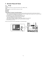
Jum per connector to connect to SC50 connector on SC board
Part number:
TZSC09187
How to use:
Caution: Remove SC jig from SC board after inspection.
1. Remove all connector between SC board and SU/SD board to isolate SC board from both SU and SD board electrically.
Note: The board will be damaged if all connector is not removed (for example; remove connector only for SU board and stay
connecting with SD board. The board will be damaged.)
2. Connect SC jig to connector SC50 at left bottom side of SC board
3. Turn of the TV/Display Unit and confirm the power LED blinking.
LED blinking: Possible cause of failure is in SC board
No LED blinking (Lighting or no lighting): Possible cause of failure is in SU or SD board
4. A fter inspection, turn off the TV/Display Unit and w ait a few minutes to discharge.
5. Remove SC jig from SC board.
Remark: This SC jig can be used for all 2009 Plasma TV and Plasma Display.
19
Summary of Contents for Viera TX-P42G15E
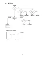
Page 17: ...6 4 No Picture No Picture Check NG 17...
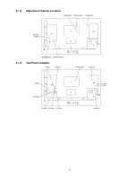
Page 31: ...9 1 4 9 1 5 Adjustment Volume Location Test Point Location 31...
Page 36: ...36...
Page 37: ...10 Block Diagram 10 1 Main Block Diagram 3 D IG IT A L S IG N A L P R O C E S S O R 37...
Page 38: ...10 2 Block 1 5 Diagram 38 0 0...
Page 40: ...10 4 Block 3 5 Diagram F O R M A T C O N V P L A S M A AI FOR FACTORY USE 40...
Page 44: ...11 3 Wiring 2 44...
Page 45: ...11 4 Wiring 3 45...
Page 46: ...U U U U D i 11 5 Wiring 4 46...
Page 47: ...11 6 Wiring 5 47...
Page 48: ...11 7 Wiring 6 48...
Page 49: ...11 8 Wiring 7 49...
Page 50: ...50...
Page 51: ...11 10 Wiring 9 51...
Page 52: ...52...
Page 55: ...12 2 P Board 1 2 Schematic Diagram A B C D E F 1 2 3 4 5 6 7 54...
Page 56: ...12 3 P Board 2 2 Schematic Diagram 55...
Page 60: ...12 7 A Board 3 22 Schematic Diagram IC 8002 MN2WS0058 19 2 0 21 2 2...
Page 64: ...V 42 43 44 45...
Page 66: ...A BO AR D 6 22 P e a ks M O D E L R EF N o 8 0 0 0 8 9 9 9 TO 5 22 TO 5 16 22 5 1 53 54...
Page 72: ...67...
Page 74: ...105 106 107 108...
Page 76: ...5 I AVSW5V1 113 114 115 116 117 69...
Page 78: ...V ID E O DET V ID E O IN 122 123 124 125 126 70...
Page 80: ...131 132 133 134 135 71...
Page 84: ...158 159 160 161 162 74...
Page 88: ...STB3 3V Q5431 185 186 187 188 189 77...
Page 90: ...SUB6v IC 2802 194 195 196 197 198 78...
Page 91: ...12 27 D Board 1 4 Schematic Diagram 79...
Page 92: ...12 28 D Board 2 4 Schematic Diagram 80...
Page 95: ...12 31 C1 Board 1 2 Schematic Diagram D A C1 BOARD TNPA4762 1 2 1 2 3 4...
Page 96: ...PANEL DATA DRIVER 5 1 6 1 7 1 8 1 9 83...
Page 101: ...12 36 SC Board 2 4 Schematic Diagram 10 11 12 13 14 15 16 17 18 88...
Page 102: ...12 37 SC Board 3 4 Schematic Diagram 19 1 20 1 21 1 22 1 23 1 24 1 25 1 26 1 27 89 C D...
Page 103: ...12 38 SC Board 4 4 Schematic Diagram 28 29 30 31 32 33 34 35 36 90...
Page 110: ...P BOARD COMPONENT SIDE ETX2MM747MFF 6 5 4 3 2 1 A I B I C I D I E I F I G I H I I 95...
Page 117: ...D BOARD COMPONENT SIDE TZTNP02DTUE 101...
Page 121: ...13 8 SC Board SC BOARD FOIL SIDE TNPA4844AH A D...
Page 122: ...104...
Page 125: ...6 SC BOARD COMPONENT SIDE TNPA4844AH 5 4 3 2 1 A I B I C I D I E I F I G I H I I 106...
Page 129: ...14 1 2 Packing 1 110...
Page 130: ...111...


