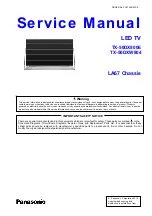
Block Diagram (2/2)
MAIN IN
P1
~
~
+
-
D7102
F7101
Li
ne
Fi
lte
r
LF7102
HOT
COLD
INV_SOS
INV_ON
INV_PWM
TV_SUB_ON
RELA
Y
16V
5VS
TUNER6V
,
2
1
Li
ne
Fi
lte
r
LF7103
PC7302
PC7303
PC7301
IC7501
T7302
2
3
1
4
2
3
1
4
2
3
1
4
IC7201
POWER
CONTROL
IC7301
PWM IC
P2
11
3,4,5
7
8
1
10
9
TO A09
Q7303
Q7302
Q7301
Q7201
T7201
5
1
3
7
6
8
9
10
7
8
3
1
R7513
Q7503
CF7101
D7809
D7808
D7807
D7806
Q7804
Q7803
D7205
D7309
D7315
D7302
D7303
D7506
R7505
Q7504
8
7
P-BOARD
IC7801
LED DRIVER
CONTROL
10
2
13
7 6
15
17
18
14
COMP
COMPSD
IS
VS
N2
PWM_IN
STB
FAIL
N1
OUT
VH
VCC
OUT
VCC
2
FB
T7801
T7802
T7803
T7804
P5
P6
P7
P8
25