


1
Applicable signals (Video/ Component/ RGB/ PC/ HDMI input
signals)
3
2
Safety Precautions
4
2.1.
General Guidelines
4
3
Prevention of Electro Static Discharge (ESD) to
Electrostatically Sensitive (ES) Devices
5
4
About lead free solder (PbF)
6
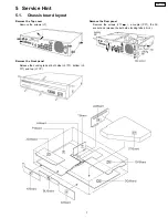
5
Service Hint
7
5.1.
Chassis board layout
7
5.2.
P.C.Board structure sheet of GP7P chassis
8
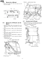
6
P.C.Board replacement method
9
6.1.
Remove the JG-Board
9
6.2.
Remove the P-Board
9
6.3.
Remove the K-Board
9
6.4.
Remove the BL-Board
9
6.5.
Remove the G-Board
10
6.6.
Remove the DT-Board and JA-Board
10
6.7.
Remove the DV Board
10
6.8.
Remove the DG-Board, T-Board and H-Board
11
7
Location of Lead Wiring
12
8
Alignment
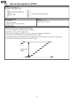
13
8.1.
Sub contrast adjustment (NTSC)
13
8.2.
Sub contrast adjustment (HDTV)
14
8.3.
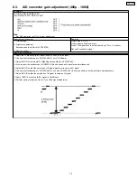
A/D converter gain adjustment (480p . 1080i)
15
9
Self-check Function
16
9.1.
Self-check of the microcomputer control system (bus line)
16
9.2.
Power LED Blinking timing chart
17
10 Serviceman Mode (Electronic Controls)
18
11 CAT (Computer Aided Test) mode
21
11.1. IIC mode
21
11.2. CD mode
22
11.3. SD mode
22
11.4. IIC mode structure (following items value is sample data.)
23
12 Circuit Board Layout
25
12.1. P-Board
25
12.2. T-Board
28
12.3. H-Board
29
12.4. DT-Board
31
12.5. JA-Board
33
12.6. DG-Board
34
12.7. DV-Board
37
12.8. BL-Board
40
12.9. G-Board
41
12.10. JG-Board
42
12.11. K-Board
44
13 Schematic Diagrams
45
13.1. Schematic Diagram Notes
45
13.2. Main Block Diagram
46
13.3. P-Board Block Diagram
47
13.4. P-Board (1 of 2) Schematic Diagram
49
13.5. P-Board (2 of 2) Schematic Diagram
50
13.6. H and T-Board Block Diagram
51
13.7. H-Board (1 of 2) and T-Board Schematic Diagram
52
13.8. H-Board (2 of 2) Schematic Diagram
53
13.9. DT and JA-Board Block Diagram
54
13.10. DT-Board (1 of 8) Schematic Diagram
56
13.11. DT-Board (2 of 8) Schematic Diagram
57
13.12. DT-Board (3 of 8) Schematic Diagram
58
13.13. DT-Board (4 of 8) Schematic Diagram
59
13.14. DT-Board (5 of 8) Schematic Diagram
60
13.15. DT-Board (6 of 8) Schematic Diagram
61
13.16. DT-Board (7 of 8) Schematic Diagram
62
13.17. DT-Board (8 of 8) Schematic Diagram
63
13.18. JA-Board Schematic Diagram
64
13.19. DG-Board Block Diagram
65
13.20. DG-Board (1 of 5) Schematic Diagram
67
13.21. DG-Board (2 of 5) Schematic Diagram
68
13.22. DG-Board (3 of 5) Schematic Diagram
69
13.23. DG-Board (4 of 5) Schematic Diagram
70
13.24. DG-Board (5 of 5) Schematic Diagram
71
13.25. DV-Board Block Diagram
72
13.26. DV-Board (1 of 5) Schematic Diagram
74
13.27. DV-Board (2 of 5) Schematic Diagram
75
13.28. DV-Board (3 of 5) Schematic Diagram
76
13.29. DV-Board (4 of 5) Schematic Diagram
77
13.30. DV-Board (5 of 5) Schematic Diagram
78
13.31. JG-Board Block Diagram
79
13.32. JG-Board (1 of 2) Schematic Diagram
80
13.33. JG-Board (2 of 2) Schematic Diagram
81
13.34. G, K and BL-Board Block Diagram
82
13.35. G, K and BL-Board Schematic Diagram
83
14 Parts Location
85
15 Mechanical Replacement Parts List
86
16 Replacement Parts List
87
Note:
Design and specifications are subject to change without notice. Weight and Dimensions shown are approximate.
CONTENTS
Page
Page
2
TU-PT700U


