background image

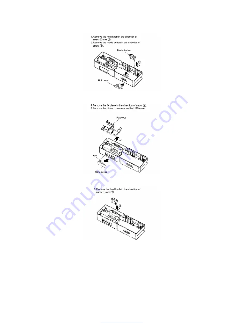
5.9. Removal of the USB fix piece and USB cover

5.10. Removal of the REC button

5.11. Removal of the tuner P.C.B. and MIC ass’y

9

PDF created with pdfFactory Pro trial version 

www.pdffactory.com

Summary of Contents for SV-MP720VGC

Page 1: ...3 Digital Audio Player SV MP720VGC SV MP720VGK SV MP720VGH SV MP720VGD SV MP720VGN Colour W White Type K Black Type SPECIFICATIONS Specifications 1 PDF created with pdfFactory Pro trial version www pdffactory com ...

Page 2: ...rs FM RADIO Approximate recording times 9 hours IC RECORDER HQ mode 5 hours FM RADIO Cabinet dimensions WxHxD 70 0 x 22 2 x 14mm Mass 36 2g with battery 23 5g without battery AC adaptir input AC110V 240V 50 Hz 60 Hz Power consumption in standby mode 0 2W Specifications are subject to change without notice The play times shown depend on operating conditions Mass and dimensions are approximate MB me...

Page 3: ...eo earphones L0BAB0000188 1pc USB Cable K1HA05AD0003 1pc Neck Strap RFAT0006 Q 1pc CD ROM Driver RFET0002 1pc AC Adaptor N0JZCD000001 GK N0JZCD000002 GD 3 PDF created with pdfFactory Pro trial version www pdffactory com ...

Page 4: ...chargeable Battery ZBRP BP65HE to be supplied will be provided with Carrying Case RFCT0005 H No replacement parts will be supplied for Rechargeable Battery without Case Replacement parts will be supplied for Carrying Case RFCT0005 H without Rechargeable Battery To your customers delivery Rechargeable Battery together with Carrying Case to prevent shorting accidents that may occur when Rechargeable...

Page 5: ...or printed circuit boards and replacing the main components 2 For reassembly after operation checks or replacement reverse the respective procedures special ressembly procedures are described only when required 3 Select item from the following index when checks or replacement are required Contents 1 Checking for the main P C B 2 Checking for the memory P C B 3 Checking for the tuner P C B 4 Checki...

Page 6: ...5 2 Removal of the front cabinet 5 3 Removal of the memory P C B 5 4 Removal of the main P C B 6 PDF created with pdfFactory Pro trial version www pdffactory com ...

Page 7: ...5 5 Removal of the battery terminal 5 6 Removal of the LCD Ass y 7 PDF created with pdfFactory Pro trial version www pdffactory com ...

Page 8: ...5 7 Removal of the LCD Piece 5 8 Removal of the mode button and hold knob 8 PDF created with pdfFactory Pro trial version www pdffactory com ...

Page 9: ...5 9 Removal of the USB fix piece and USB cover 5 10 Removal of the REC button 5 11 Removal of the tuner P C B and MIC ass y 9 PDF created with pdfFactory Pro trial version www pdffactory com ...

Page 10: ...6 Instructions for Repair Service 7 Service Position 10 PDF created with pdfFactory Pro trial version www pdffactory com ...

Page 11: ...8 Service Mode 8 1 Checking Procedures for IC3 C2HBZG000008 11 PDF created with pdfFactory Pro trial version www pdffactory com ...

Page 12: ...8 2 Checking Procedures for Font table 12 PDF created with pdfFactory Pro trial version www pdffactory com ...

Page 13: ...ter replacing the main PCB and DSP IC main CPU reinstall DFU and firmware and copy font table again 9 2 Please contact to the service organization of the belonging for the acquisition of data and obtain the software 13 PDF created with pdfFactory Pro trial version www pdffactory com ...

Page 14: ...14 PDF created with pdfFactory Pro trial version www pdffactory com ...

Page 15: ...15 PDF created with pdfFactory Pro trial version www pdffactory com ...

Page 16: ...ows Media Player V9 0 installed Be sure to check for normal operation of the PC If other application software is installed in the PC be sure that this software does not affect the operation of the Windows Media Player V9 0 16 PDF created with pdfFactory Pro trial version www pdffactory com ...

Page 17: ...daptor can be connected properly There is a possibility that not only the hardware but also software PC s application software may be the source of the problem Therefore be sure to inspect all potential sources carefully and thoroughly before specifying any causes Remarks When the PC does not recognize the USB reader writer as a removable disc even when the USB reader writer is connected to the PC...

Page 18: ...s unit away from mobile telephones Play doesn t resume from the track where I stopped play This doesn t work if You download record or delete files or charge the battery The random play mode is on Play doesn t start from the first track The random play mode may be on Play usually resumes from the track where you last stopped play Use skip to return to the first track The unit stops working Take th...

Page 19: ...duct itself This schematic diagram may be modified at any time with the development of new technology S1 PLAY STOP switch S2 FF switch S3 REW switch S4 Volume up switch VOL S5 Volume down switch VOL S6 REC switch S7 MODE switch S8 HOLD switch HOLD The supply part number is described alone in the replacement parts list Voltage from negative terminal of battery MP3 position FM position No mark MP3 A...

Page 20: ...ts list Caution IC and LSI are sensitive to static electricity Secondary trouble can be prevented by taking care during repair Cover the parts boxes made of plastics with aluminum foil Ground the soldering iron Put a conductive mat on the work table Do not touch the legs of IC or LSI with the fingers directly 15 Schematic Diagram 16 Printed Circuit Board Diagram 17 Cabinet Parts Location 20 PDF cr...

Page 21: ...18 Packaging 21 PDF created with pdfFactory Pro trial version www pdffactory com ...

Page 22: ...nts identified by mark have special characteristics important for safety Furthermore special parts which have purposes of fire retardant resistors high quality sound capacitors low noise resistors 22 PDF created with pdfFactory Pro trial version www pdffactory com ...

Page 23: ...BLY Black T K2 ZA4MP720VGKW DOWM CABINET ASSEMBLY White T K3 RKKT0058 K BATTERY COVER Black T K3 RKKT0059 W BATTERY COVER White T K4 RGUT0209 1S1 REC BUTTON T K5 RGVT0092 K HOLD KNOB Black T K5 RGVT0092 W HOLD KNOB White T K6 RGUT0208 K MODE BUTTON Black T K6 RGUT0208 W MODE BUTTON White T K7 RMNT0099 K JACK USB FIX PIECE Black T K7 RMNT0099 W JACK USB FIX PIECE White T K8 RXQT0006 1S USB COVER AS...

Page 24: ... GC RQTT0663 R INSTRUCTION BOOK T A10 GC RQTT0720 R INSTRUCTION BOOK T PACKING MATERIALS P1 GC RPKT0796 1 DECORATION BOX Black T P1 GC RPKT0898 1 DECORATION BOX White T P1 GK RPKT0797 DECORATION BOX Black T P1 GK RPKT0900 DECORATION BOX White T P1 GD RPKT0798 1 DECORATION BOX Black T P1 GD RPKT0901 1 DECORATION BOX White T P1 GN RPKT0799 1 DECORATION BOX Black T P1 GN RPKT0902 1 DECORATION BOX Whi...

Page 25: ...INDUCTOR T L5 J0JBC0000044 CHIP COIL T L6 J0JBC0000044 CHIP COIL T L7 G1A220C00006 POWER INDUCTOR T L8 G1A220C00006 POWER INDUCTOR T L10 G1A220C00006 POWER INDUCTOR T L11 J0JBC0000044 CHIP COIL T L12 J0JBC0000044 CHIP COIL T L13 J0JBC0000044 CHIP COIL T L14 J0JBC0000044 CHIP COIL T L15 J0JBC0000044 CHIP COIL T L16 J0JBC0000044 CHIP COIL T L19 J0JBC0000044 CHIP COIL T L20 J0JBC0000044 CHIP COIL T L...

Page 26: ...0 PIN CONNECTOR HEADER T CN6 K1KB24A00045 24 PIN CONNECTOR HEADER T RESISTORS R1 D0GAR00JA020 CHIP RESISTOR T R2 D0GAR00JA020 CHIP RESISTOR T R3 D0GA100JA020 CHIP RESISTOR T R4 D0GA183JA020 CHIP RESISTOR T R5 D0GAR00JA020 CHIP RESISTOR T R6 D0GA104JA020 CHIP RESISTOR T R7 D0GA103JA020 CHIP RESISTOR T R8 D1H42202A014 CHIP RESISTOR T R11 D0GA332JA020 CHIP RESISTOR T R12 D0GA472JA020 CHIP RESISTOR T ...

Page 27: ...ISTOR T R301 D1H41042A014 CHIP RESISTOR T R303 D0GA474JA020 CHIP RESISTOR T R304 D0GA104JA020 CHIP RESISTOR T R307 D0GA100JA020 CHIP RESISTOR T R308 D0GA100JA020 CHIP RESISTOR T R309 D0GB470JA008 CHIP RESISTOR T R310 D0GB102JA008 CHIP RESISTOR T R311 D0GB470JA008 CHIP RESISTOR T R312 D0GB470JA008 CHIP RESISTOR T CHIP JUMPERS J5 D0GBR00JA008 CHIP RESISTOR T J11 D0GAR00JA020 CHIP RESISTOR T J13 D0GA...

Page 28: ...A451 CHIP CAPACITOR T C42 K105BJ104KVC CHIP CAPACITOR T C43 K105BJ104KVC CHIP CAPACITOR T C44 K105BJ104KVC CHIP CAPACITOR T C45 K105BJ104KVC CHIP CAPACITOR T C46 K105BJ104KVC CHIP CAPACITOR T C50 K105BJ104KVC CHIP CAPACITOR T C51 RCST0GY686RU TANTALUM CAP T C55 F3E0G226A002 TANTALUM CAP T C56 ECUENA473KBQ CHIP CAPACITOR T C57 ECUVNA105ZFV CHIP CAPACITOR T C58 ECUVNA105ZFV CHIP CAPACITOR T C59 ECUV...

Page 29: ...CST0JZ106R TANTALUM CAP T C202 K105BJ104KVC CHIP CAPACITOR T C203 K105BJ104KVC CHIP CAPACITOR T C204 ECST0JZ106R TANTALUM CAP T C205 ECUE1H060DCQ CHIP CAPACITOR T C206 ECUE1H060DCQ CHIP CAPACITOR T C301 ECST0JZ106R TANTALUM CAP T C303 F1H1C104A071 CHIP CAPACITOR T C304 ECUVNA105ZFV CHIP CAPACITOR T C305 F3H0G107A062 TANTALUM CAP T C306 F3H0G107A062 TANTALUM CAP T C307 F3H0G107A062 TANTALUM CAP T C...

Page 30: ...l FM Signal Rec Signal IC 1 FM Tuner IC3 DSP MP3 Decoder FM Demodulator IC Recoder FM Signal IC2 Flash memory 12MHz Clock USB port Control Headphone IC4 EL Drive MIC DC DC Conv IC 7 8 AC Adaptor Battery LCD Display 13MHz Clock Rec Signal ...

Page 31: ...AIN AGND V CCD RFI 1 RF GND RFI 2 TAGC CP OUT VCO TANK1 VCO TANK2 VCC VCO DGND VCCD DATA CLOCK BUSENABLE BUSMODE SWPORT1 SWPORT1 XTAL1 XTAL2 LIMDEC1 LIMDEC2 TIFC Vref MPXO TMUTE VAFR VAFL PILFIL PHASEFIL GAIN STABILIZTION RESONANCE AMPLIFIER LIMITER DEMODULATOR POWER SUPPLY SOFT MUTE MPX DECODER CRYSTAL OSCILLATOR SOFTWARE PROGRAMMABLE PROT I O MIXER 1st FM AGC N1 2 TUNING SYSTEM VCO IF CENTER FRE...

Page 32: ...ch also increments the internal column address counter by one CE CHIP ENABLE The CE input is the device selection control When the device is in the Busy state CE high is ignored and the device does not return to standby mode in program or erase opertion Regarding CE control during read operation refer to Page read section of Device operation CLE COMMAND LATCH ENABLE The CLE input controls the acti...

Page 33: ...LCD_DB_6 LCD_DB_1 LCD_DB 3 LCD_DB_2 LCD_RS high Data register selsct low Instruction register select LCD_DB 0 LCD_CSB Chip Select T1 T4 N1 N2 T10 V9 F3 C2 B3 C1 C3 D2 D1 D3 E2 E3 F2 G2 R3 X2 12MHz 15 3 3V VDD IC7 DC DC CONV IC4 EL DRIVER D18 ADC_MIC Microphone Input BATTERY 1 2V J17 USB_DP Positive USB data line usb 2 0 FS USB_DM Negative USB data line usb 2 0 FS USB_RPU Soft connect output usb 2 ...

Page 34: ...000008 V15 MPMC A12 A17 C9 E18 D16 D18 A14 B14 A13 B13 A1 A2 B2 A3 A4 B4 A5 B5 U5 T6 U6 T7 U7 V10 U10 U3 V3 T3 U2 V1 V2 T1 T4 U1 R3 T2 M3 M2 L1 L2 M1 P3 N3 N2 N1 R1 R2 P2 P1 H16 J17 T15 U17 T17 U14 P16 R17 R16 T16 U15 U16 U18 V18 G2 F2 E3 E2 D3 D1 D2 C3 C1 C2 B3 F3 Micro Processor Unit MPU AHB Advanced High Performance Bus Digital Audio Codec Multi Purpose Memory Control Fiash Memory Control Data ...

Page 35: ...thode B0CCAA000001 A Ca Anode Cathode MA2Z74800L 4 3 5 2 1 XC6367A333MR 4 3 2 1 XC6213B282NR XC61CN1602NR B1ADMB000012 2SA1774STL UN9115JTX D G S B1CFMC000005 C B C E B C B E UMX1NTN E B0JDDB000002 Anode Cathode Anode B0ACEM000008 B0ZBZ0000070 A Ca Anode A Anode 46 1 90 91 135 136 180 45 ...

Page 36: ...ing the AC adaptor Recharging also takes place when the player is connected to a computer s USB port Operation cannot be guaranteed if you use a USB hub or extension cable 2 Recharging time Approx 6 hours The display will turn off when recharging is complete 1 2 3 To a household mains socket AC Adaptor Insert so the arrow is facing upwards Connecting to a computer and downloading files 4 3 2 To US...

Page 37: ...3 R16 R12 R18 C103 R30 C20 E C B R11 D5 R14 R13 SW7 D3 Q3 R21 E C B R39 MODE A B C D E F G H 6 5 4 3 2 1 TUNER P C B SIDE A A TUNER P C B SIDE B A C92 R4 R22 R3 L30 C91 L27 L1 R6 C73 R75 C3 L4 1 L3 C8 C7 C4 C6 L5 L2 C9 X1 R27 R31 R8 R2 R1 IC6 IC1 C14 C15 R7 D1 D2 C5 C10 C12 C11 C13 C17 C18 2 3 4 15 5 11 10 1 21 20 30 25 40 35 31 C19 C21 C22 C23 C24 L26 C16 BATTERY TERMINAL To MAIN C P C B CN2 C68 ...

Page 38: ... C99 CN4 IC7 BATTERY 1 2V To MEMORY B P C B CN5 To TUNER A P C B CN6 To TUNER P C B A BATTERY TERMINAL Note This printed circuit board diagram may be modified at any time with the development of new technology Q7 IC9 IC10 X2 ICP1 1 2 3 4 1 2 3 4 1 2 3 4 5 ON OFF E C B E C B TP2 TP12 C105 R32 SV MP720V GC GK GH GD GN MAIN P C B C201 C204 L202 L201 C203 C202 C110 R205 C115 R201 R34 C306 C305 C308 L4...

Page 39: ...C W R LGAIN AGND VCCD RFI 1 RF GND RFI 2 TAGC LOOP SW CP OUT VCOTANK1 VCOTANK2 VCC VCO DGND VCCD DATA CLOCK BUSENABLE BUSMODE SWPORT1 SWPORT1 XTAL1 XTAL2 LIMDEC1 LIMDEC2 TIFC Vref MPXO TMUTE VAFR VAFL PILFIL PHASEFIL D2 D1 B0CCAA000001 B0CCAA000001 L3 L4 C14 K0 022 C15 K0 022 G1C33NJA0037 G1C33NJA0037 L2 R3 10 C1 K0 1 C2 4V22 C9 Z1 0 1 2 3 4 VIN VOUT CE VSS IC6 C16 Z1 0 C0CBCAC00288 A B C D E F G ...

Page 40: ...2 94 0 0 3 0 0 0 0 3 0 3 0 0 0 0 0 0 0 0 0 0 1 2 0 0 1 2 1 2 1 2 0 0 0 0 3 0 1 2 1 2 1 2 1 2 0 0 0 0 0 0 0 R39 100K 15 14 5 7 9 11 13 12 10 8 6 3 4 1 2 17 16 19 18 21 20 23 22 24 Q2 CN5 30 28 29 26 27 25 C20 4V100 SW7 MODE SW5 VOL SW1 PLAY SW2 FF SW3 REW R11 3 3K R12 4 7K R13 6 8K SW4 VOL R14 10K R15 22K R16 68K R21 680 R20 1 5 R23 27 R25 27 Q3 B1ADMD000012 D3 MA3J14700L R30 18K D5 B0JDDB000002 7 ...

Page 41: ...4 5 6 Schematic diagram 3 A B E F G H J N B5 A5 B4 A4 A1 G16 B2 A2 A3 B14 Y A13 K L D L34 L33 L42 L41 J5 0 C ADAPTOR IN VCC 5V VDD D8 C100 Z1 0 C99 4V22 L39 L38 L35 C101 K1 0 IC10 C0CBCAC00288 1 2 3 4 VIN VOUT CE VSS R66 4 7K C105 K330P IC9 C0EBC0000204 4 3 2 1 VIN VOUT NC VSS R71 330K R68 4 7K R69 180K R70 22K K2 A1 ICP1 MAIN CIRCUIT C TP12 Q7 UMX1NTN Chargeable Control RESET IC REGULATOR L31 3 0...

Page 42: ...C_SDA IIC_SCL USB_DP USB_DM USB_RPU USB_GNDA USB_VBUS USB_RREF USB_VDDA18_BG USB_VDDA18_PLL USB_VSSA_TEEM USB_VSSA_REF USB_VDDA33 USB_VDDA33 DRV GPIO_3 GPIO_2 GPIO_1 GPIO_0 RSTIN_N DC_DC_PLAY DC_DC_STOP DC_DC_LX2 DC_DC_LX1 DC_DC_VUSB DC_DC_VBAT DC_DC_VOUT33A DC_DC_VOUT33B DC_DC_VOUT18 DC_DC_VSS1 DC_DC_VSS2 DC_DC_GND DC_DC_CLEAN ADC10B_GPA4 ADC10B_GPA3 ADC10B_GPA2 ADC10B_GPA1 ADC10B_GPA0 ADC10B_VDD...

Page 43: ...TP3 A B C D E F G H 13 14 15 16 17 18 G L D H J E F A B C D E F G H I J K L A B N IC7 C0DBAGZ00021 4 5 1 3 2 VDD VOUT CE EXT GND C Q8 B1CFMC00005 L8 C96 K0 1 C97 K0 1 C95 4V100 D6 K2 A1 C104 K0 1 L37 R73 0 Schematic diagram 5 MAIN CIRCUIT C EL DRIVER DC DC CONV DC DC CONV 0 0 3 23 1 33 0 0 3 26 1 33 AC 83V AC 82V 3 08 1 18 3 26 1 33 0 1 38 0 3 26 1 36 3 26 1 36 3 0 0 1 38 0 0 1 40 1 45 C310 0 47 C...

Reviews: