background image

81

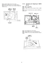
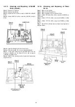
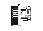
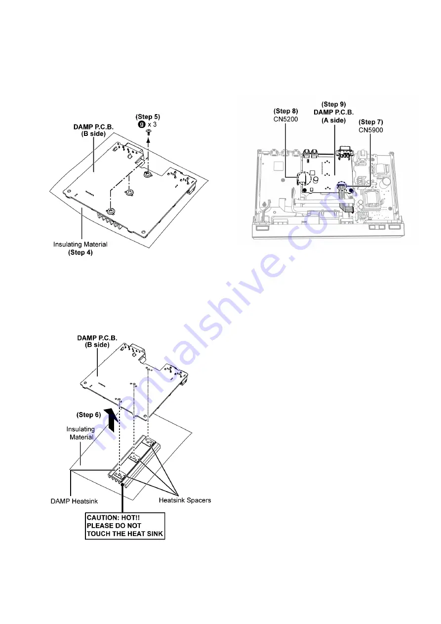
12.1.4. Checking and Repairing of DAMP

P.C.B. (Side A)

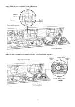
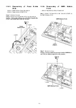
Step 1 :

 Remove Top Cabinet.

Step 2 :

 Remove Rear Panel.

Step 3 :

 Remove the DAMP P.C.B..

Step 4 :

 Place the DAMP P.C.B. on an Insulated Material.

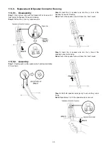
Step 5 :

 Remove 3 screws.

Step 6 :

 Lift up the DAMP P.C.B. as arrow shown.

Caution 1: Keep the Heatsink Spacer in safe place. Avoid 

denting it, place it back during assembling.

Caution 2: Handle the DAMP Heatsink & P.C.B. with caution 

due to it’s high temperature after prolonged use. Touching 

it may lead to injuries.

Step 7 :

 Attach 6P Cable Wire at the connector (CN5900) on

DAMP P.C.B..

Step 8 :

 Attach 40P FFC at the connector (CN5200) on DAMP

P.C.B..

Step 9 :

 DAMP P.C.B. (A side) can be checked and repaired as

diagram shown.

Summary of Contents for SU-HTB550GK

Page 1: ...Black Type TABLE OF CONTENTS PAGE PAGE 1 Safety Precautions 3 1 1 General Guidelines 3 1 2 Before Repair and Adjustment 4 1 3 Protection Circuitry 4 1 4 Caution For Fuse Replacement 4 1 5 Caution For SMPS Module 4 1 6 Caution for the AC Mains Lead For GS only 5 1 7 Safety Part Information 6 1 8 Safety Installation Instructions 7 2 Warning 8 2 1 Prevention of Electro Static Discharge ESD to Electro...

Page 2: ...oofer SB HWA520 83 13 Overall Simplified Block 85 13 1 Overall Control Diagram 85 13 2 Power Supply Diagram 86 14 Block Diagram 87 14 1 SYSTEM CONTROL BLOCK DIAGRAM 87 14 2 HDMI BLOCK DIAGRAM 88 14 3 AUDIO BLOCK DIAGRAM 89 14 4 IC TERMINAL CHART 90 14 5 POWER SUPPLY 1 2 BLOCK DIAGRAM 91 14 6 POWER SUPPLY 2 2 BLOCK DIAGRAM 92 14 7 AUDIO POWER SUPPLY BLOCK DIAGRAM 93 15 Wiring Connection Diagram 94 ...

Page 3: ... exposed metal does not have a return path to the chassis the reading must be 1 1 2 Leakage Current Hot Check 1 Plug the AC cord directly into the AC outlet Do not use an isolation transformer for this check 2 Connect a 1 5kΩ 10 watts resistor in parallel with a 0 15μF capacitors between each exposed metallic part on the set and a good earth ground such as a water pipe as shown in Figure 1 3 Use a...

Page 4: ...220 mA For GK Current consumption at AC 110 240V 50 60 Hz in Power On link Volume minimum SEL DVD mode should be 220 mA For GS GXS 1 3 Protection Circuitry The protection circuitry may have operated if either of the following conditions are noticed No sound is heard when the power is turned on Sound stops during a performance The function of this circuitry is to prevent circuitry damage if for exa...

Page 5: ...5 1 6 Caution for the AC Mains Lead For GS only ...

Page 6: ...6AD MAIN TRANSFORMER PC5720 B3PBA0000503 PHOTO COUPLER PC5760 B3PBA0000503 PHOTO COUPLER F1 K5G312Y00007 FUSE TH5702 D4CAA5R10001 THERMISTOR P5701 K2AA2B000011 AC INLET R5700 ERJ8GEYJ105V 1M 1 4W R5701 ERJ8GEYJ105V 1M 1 4W R5710 ERJ8GEYJ105V 1M 1 4W C5700 F1BAF471A013 470pF C5701 F0CAF104A105 0 1uF C5702 F0CAF104A105 0 1uF C5703 F0CAF104A105 0 1uF C5705 F1BAF1020020 1000pF GK C5705 F1BAF471A013 47...

Page 7: ...7 1 8 Safety Installation Instructions ...

Page 8: ...osure of the assembly 3 Use only a grounded tip soldering iron to solder or unsolder ES devices 4 Use only an anti static solder remover device Some solder removal devices not classified as anti static ESD protected can generate electrical charge to damage ES devices 5 Do not use freon propelled chemicals These can generate electrical charges sufficient to damage ES devices 6 Do not remove a repla...

Page 9: ...is used Definition The letter of PbF is printed on the PCB using the lead free solder To put lead free solder it should be well molten and mixed with the original lead free solder Remove the remaining lead free solder on the PCB cleanly for soldering of the new IC Since the melting point of the lead free solder is higher than that of the normal lead solder it takes the longer time to melt the lead...

Page 10: ... the circuit is changed or modified this information will be followed by supplement service manual to be filed with original service manual Microprocessor The following components are supplied as an assembled part Microprocessor IC IC2301 RFKWMHTB550P SMPS Module Active Subwoofer SB HWA520 uses SMPS Module to supply the voltage power required for the circuitries It is replaced as an assembly do no...

Page 11: ... Power supply AC 220 V 50 Hz For GK AC 110 V to 240 V 50 60 Hz For GS GSX Dimensions W x H x D Main Unit Cabinet dimension 310 mm x 44 mm x 195 mm Maximum outer dimension 310 mm x 45 mm x 202 mm Active subwoofer 180 mm x 408 mm x 306 mm Mass Weight Main Unit 1 1 kg Active subwoofer 5 2 kg Operating temperature range 0 C to 40 C Operating humidity range 20 to 80 RH no condensation Q Speaker general...

Page 12: ...12 5 General Introduction 5 1 About VIERA Link ...

Page 13: ...and worldwide patents issued pending DTS the Symbol DTS and the Symbol together are registered trademarks DTS Digital Surround and the DTS logos are trademarks of DTS Inc Product includes software DTS Inc All Rights Reserved HDMI the HDMI Logo and High Definition Multimedia Interface are trademarks or registered trademarks of HDMI Licensing LLC in the United States and other countries HDAVI Contro...

Page 14: ...is the audio source 6 Audio format indicators 1 Dolby Digital indicator Lights when Dolby Digital is the current audio format DTS indicator Lights when DTS is the current audio format PCM indicator Lights when PCM 2ch Multi channel is the current audio format 7 WIRELESS LINK indicator 1 AC IN terminal 2 Speaker terminals 3 TV terminal 4 AUX2 terminal 5 HDMI OUT terminal ARC compatible 6 BD DVD ter...

Page 15: ...dio setting is Main When the auto gain control is on When 3D surround effect and clear mode dialog effect are on When the auto standby function is on The indicators blinks for 10 sec When the dialog effect level or the subwoofer level is 2 When the audio output mode is Auto mode The indicator blinks for 10 sec When the audio output mode is Auto mode The indicators blinks for 10 sec When the dialog...

Page 16: ... DVD as the source 8 Select the AUX as the source AUX1 AUX2 DIALOGLEVEL BD DVD 1 6 7 2 3 4 5 8 AUX Remove the insulation sheet before using To replace a button type battery While pressing the stopper pull out the battery holder Set the button type battery with its mark facing upward and then put the battery holder back in place When replacing the battery use CR2025 Lithium battery Keep the button ...

Page 17: ...main unit to the terminal labeled HDMI ARC the optical digital audio cable that is usually required in order to listen to sound from a TV is no longer required and TV pictures and sound can be enjoyed with a single HDMI cable Make the connection Connection differs depending on the label printed next to the HDMI terminal Labeled HDMI ARC Connection Not Labeled HDMI ARC Connection A B Labeled HDMI A...

Page 18: ...astly selected is output 3D compatibility Compatible with FULL HD 3D TV and Blu ray Disc player TM The main unit can pass the 3D video signal from a 3D compatible Blu ray Disc player TM to a FULL HD 3D TV When the device has an HDMI terminal HDMI cable When the device has an optical digital audio output terminal Refer to the operating instructions of the respective devices for the optimal connecti...

Page 19: ...or the area you live in In Saudi Arabia please use the moulded three pin mains plug The main unit and active subwoofer consume a small amount of AC power even when it is turned off this unit approx 0 2 W active subwoofer approx 0 2 W In the interest of power conservation if you will not be using this system for a long time unplug it from the household mains socket When using the moulded three pin ...

Page 20: ...lay Details by LED Blinking Indicators Caution The LED blinking process will stop only when the unit is power off completely Table 8 1 1 Remote Control Code LED 1 TV LED 2 BD DVD LED 3 AUX1 LED 4 AUX2 LED 5 DOLBY D LED 6 DTS LED 7 PCM Test Mode and Purpose TV O ERROR HISTORY DISPLAY By pressing button it goes back its history list Eg 1 F76 2 F70HDM 3 F61 INPUT AUX O Accumulation Operation Time Dis...

Page 21: ...peated every 16 releases Table 8 1 2 1 8 1 2 2 Region Bit No The region bit no is to indicate the destination for model Refer to table 8 1 2 2 for more information Table 8 1 2 2 Key Operation LED 1 TV LED 2 BD DVD LED 3 AUX1 AUX LED 4 AUX2 LED 5 DOLBY D LED 6 DTS LED 7 PCM AAC Press VOL button on remote control for one times O X Bit 3 X Bit 2 Bit 1 Bit 0 Press VOL button on remote control for two ...

Page 22: ... 8 1 3 8 1 3 1 Model Display It is to indicate the model display Refer to table 8 1 3 1 for more information Table 8 1 3 1 8 1 3 2 ROM Correction Display It is to indicate the ROM correction display Refer to table 8 1 3 2 for more information Table 8 1 3 2 Key Operation LED 1 TV LED 2 BD DVD LED 3 AUX1 AUX LED 4 AUX2 LED 5 DOLBY D LED 6 DTS LED 7 PCM AAC Press VOL button on remote control for one ...

Page 23: ... 5 DOLBY D LED 6 DTS LED 7 PCM Cause and Problem OVERLOAD F61 If this error occurs main set will automatically power off X X X X X Speaker protection DAMP IC abnormality Check for faulty parts and replace with new parts if necessary F76 If this error occurs main set will automatically power off X X X X X X DC Power Voltage Supply abnormality Check for faulty parts and replace with new parts if nec...

Page 24: ... LED blinking press INPUT or AUX on remote control followed by VOL on Main Unit for 2 secs Pairing begins Note 1 Under Pairing Mode BD DVD LED blinking and 3 indicators LEDs Dolby D DTS and PCM AAC will run one by one shifting for every 1 sec from left to right to indicate it is searching for the receiver to be linked and repeated the cycle after reached the AAC or PCM LED 2 When pairing is comple...

Page 25: ... IC5801 LED display checking Check the display by Doctor Mode Some not lighting not light off Failure of drive IC Failure of not lights up LED Check Panel IC6001 5 6 7 8 9 10 LED㸸ONĺ0V OFFĺ5V All not lighting Checking the drive IC serial signal FFC Check Panel IC6001 18 ĺ3 3VࠊD6001 Anode ĺ5V Check Panel IC6001 2 3 4 serial signal Video confirmation No audio output when video on Even change the HDM...

Page 26: ...26 ...

Page 27: ...xture Tools Prepare service tools before process service position Ref No Service Tools Remarks SFT1 Main P C B CN2201 DAMP P C B CN5200 RFKZHTB15 40P FFC SU HTB550 SFT2 SPK DAMP P C B CN1005 REXX1194 2P Wire SB HWA520 ...

Page 28: ... following indexes when disassembly or replacement are required Main Unit SU HTB550 Disassembly of Top Cabinet Disassembly of Main P C B Disassembly of SMPS P C B Replacement of Switching Regulator IC IC5701 Replacement of Rectifier Diode D5802 Disassembly of Rear Panel Disassembly of DAMP P C B Disassembly of Front Panel Block Disassembly of Wireless Adapter P C B and Digital Transmitter Module P...

Page 29: ...hart is the procedure for disassembling the casing and inside parts for internal inspection when carrying out the ser vicing To assemble the unit reverse the steps shown in the chart below 11 1 1 Main Unit SU HTB550 11 1 2 Front Speakers SB HTB550 ...

Page 30: ...30 11 1 3 Active Subwoofer SB HWA520 ...

Page 31: ...31 11 2 Types of Screws 11 2 1 Main Unit SU HTB550 11 2 2 Front Speakers SB HTB550 11 2 3 Active Subwoofer SB HWA520 ...

Page 32: ...32 11 3 Main Parts Location Diagram 11 3 1 Main Unit SU HTB550 11 3 2 Front Speakers SB HTB550 11 3 2 1 Bar Position ...

Page 33: ...33 11 3 2 2 Standing Position 11 3 3 Active Subwoofer SB HWA520 ...

Page 34: ... Step 1 Remove 2 screws Step 2 Remove 3 screws Step 3 Slightly pull outwards the Top Cabinet for both sides Step 4 Lift up the Top Cabinet to remove it as shown Caution During assembling ensure that the edge of Top Cabinet fully insert into the Front Panel Block ...

Page 35: ... 2 Detach 2P Cable Wire at the connector CN2206 on Main P C B Step 3 Detach 40P FFC at the connector CN2201 on Main P C B Step 4 Detach 17P FFC at the connector CN2205 on Main P C B Step 5 Detach 11P FFC at the connector CN2204 on Main P C B Step 6 Detach 9P FFC at the connector CN2202 on Main P C B ...

Page 36: ...36 Step 7 Remove 2 screws Step 8 Slightly lift up and remove the Main P C B as shown Caution During assembling ensure that the Main P C B is seated properly on the locators ...

Page 37: ...Step 2 Detach 6P Cable Wire at the connector CN5900 on DAMP P C B Step 3 Detach 9P FFC at the connector CN1 on SMPS P C B Step 4 Remove 4 screws Step 5 Release the guides on the right side Rear Panel slightly Caution During assembling ensure that the Rear Panel is seated properly onto the guide ...

Page 38: ...tching Regula tor IC IC5701 Refer to Disassembly of SMPS P C B 11 4 4 1 Disassembly of Switching Regu lator IC IC5701 Caution Handle the SMPS P C B with caution Avoid touching the Heatsink Unit A due to it s high temperature after prolonged use Touching it may lead to injuries Step 1 Desolder the pins of Switching Regulator IC IC5701 on the solder side of SMPS P C B ...

Page 39: ... Step 1 Apply Grease on the Heatsink Unit A Step 2 Fix the Switching Regulator IC IC5701 to the SMPS P C B Caution Ensure the pins of Switching Regulator IC IC5701 seated on the SMPS P C B Step 3 Screw the Switching Regulator IC IC5701 to the Heatsink Unit A Caution Ensure the Switching Regulator IC IC5701 is tightly screwed to the Heatsink Unit A ...

Page 40: ...4 5 1 Disassembly of Rectifier Diode D5802 Caution Handle the SMPS P C B with caution Avoid touching the Heatsink Unit B due to it s high temperature after prolonged use Touching it may lead to injuries Step 1 Desolder the pins of the Rectifier Diode D5802 on the solder side of SMPS P C B Step 2 Remove 1 screw Step 3 Remove the Rectifier Diode D5802 from the Heatsink Unit B ...

Page 41: ... D5802 onto the Heatsink Unit B with a screw Caution Ensure the Rectifier Diode D5802 is tightly screwed to the Heatsink Unit B Step 4 Solder the pins of the Rectifier Diode D5802 on the solder side of SMPS P C B 11 4 6 Disassembly of Rear Panel Refer to Disassembly of Top Cabinet Step 1 Remove 9 screws Step 2 Release the guides on both sides Caution During assembling ensure that the Rear Panel is...

Page 42: ...ly of Rear Panel Step 1 Remove 2 screws Step 2 Detach 6P Cable Wire at the connector CN5900 on DAMP P C B Step 3 Detach 40P FFC at the connector CN5200 on DAMP P C B Step 4 Remove the DAMP P C B as shown Caution During assembling ensure that the DAMP P C B is seated properly on the locators ...

Page 43: ...CN2204 on Main P C B Step 4 Release 2 catches Caution During assembling ensure that the Front Panel Block is properly inserted and fully catches onto the Bot tom Chassis Step 5 Release 3 catches Caution During assembling ensure that the Front Panel Block is properly inserted and fully catches onto the Bot tom Chassis Step 6 Release 2 guides Caution During assembling ensure that the Front Panel Blo...

Page 44: ... Transmitter Mod ule P C B Refer to Disassembly of Top Cabinet Refer to Disassembly of Front Panel Block Step 1 Remove 1 screw Step 2 Lift up the Digital Transmitter Holder Unit as shown Step 3 Release the Digital Transmitter Holder Unit from hook Step 4 Remove the Digital Transmitter Holder Unit as shown ...

Page 45: ... Step 5 Remove 1 screw Step 6 Release 2 catches Caution During assembling ensure that the Wireless Adapter P C B is seated properly onto the guides and fully catches onto the Digital Transmitter Holder Step 7 Remove the Wireless Adapter P C B and the Digital Transmitter Module P C B together as shown Caution During assembling ensure that the Digital Trans mitter Module P C B is properly inserted i...

Page 46: ...C B as direction with Shield Plate is facing to Ground Spring 11 4 10 Disassembly of Power Button P C B Refer to Disassembly of Top Cabinet Refer to Disassembly of Front Panel Block Step 1 Remove 1 screw Step 2 Remove the Stopper P C B through the 2P Cable Wire as shown Caution During assembling ensure that the Stopper P C B is seated properly onto the guides of the Front Panel Block ...

Page 47: ... C B is inserted properly into the gaps of the Front Panel Block 11 4 11 Disassembly of Button P C B and Panel P C B Refer to Disassembly of Top Cabinet Refer to Disassembly of Front Panel Block Step 1 Remove 2 screws Step 2 Lift up the Volume Button Bracket as shown Step 3 Remove the Volume Button Bracket ...

Page 48: ...ssembling ensure that the Volume But ton Bracket is seated properly on the guides of the Front Panel Block Step 4 Lift up to release the Button P C B from the slots of the Front Panel Block Caution During assembling ensure that the Button P C B is properly inserted into the slots of the Front Panel Block Step 5 Remove the Volume Button as shown ...

Page 49: ...me But ton is properly located in between the 3 ribs of the Front Panel Block Step 6 Remove 1 screw Step 7 Remove the Panel P C B as shown Caution During assembling ensure that the Panel P C B is seated properly on the guides of the Front Panel Block ...

Page 50: ...HTB550 11 5 1 Disassembly of Front Speaker Unit L R Bar position Front Speaker Unit with Stand Step 1 Remove 2 screws Step 2 Remove 2 Stands Front Speaker Unit with Support Leg Step 1 Remove 2 screws Step 2 Remove 2 Support Legs ...

Page 51: ...51 Step 3 Release the Speaker Wires from the grooves Step 4 Remove 4 screws Step 5 Detach the Front Speaker Unit L R as arrow shown ...

Page 52: ...hanical structure The same disassembly procedure can be applied for the both of them Front Speaker Unit L is illustrated here Step 1 Push and release the White and Blue Speaker wires from Terminal Step 2 Release the Speaker Wires from the groove Step 3 Release the Speaker Wires from the groove Step 4 Remove 1 screw ...

Page 53: ...53 Step 5 Remove the Speaker Base Step 6 Remove 2 screws Step 7 Push up and remove the Front Ornament Assembly ...

Page 54: ...peaker Unit L is illustrated here Refer to Disassembly of Front Speaker Unit L R Step 1 Remove 12 screws Caution During assembling ensure that the screws are fixed by following the sequence from 1 to 12 Step 2 Upset the unit Step 3 Slightly tilt and lift up the Front Cabinet Block by using screwdriver with cloth Caution Do not exert too much force as it may damage the Front Cabinet Block ...

Page 55: ...Upset the Front Cabinet Block and place by the side of the Rear Cabinet Assembly Step 6 Detach the Red and Black wires Step 7 Remove the Sound Absorber Caution Keep the Sound Absorber in safe place and place them back during assembling Step 8 Remove the Rear Cabinet Assembly ...

Page 56: ...56 Step 9 Remove 1 screw Step 10 Slightly bend up the Terminal and Terminal Step 11 Remove the Terminal as arrow shown ...

Page 57: ...disassembly procedure can be applied for the both of them Front Speaker Unit L is illustrated here Refer to Disassembly of Front Speaker Unit L R Refer to Step 1 to Step 4 of Disassembly of Rear Cabinet Assembly Step 1 Release the Speaker Wires from the ribs of the Front Cabinet Block Step 2 Detach the Black and Blue wires ...

Page 58: ...Remove 4 screws Step 4 Remove the Tweeter Speaker SP1 and Eva Packing Caution During assembling ensure that the Tweeter Speaker SP1 and Eva Packing is properly seated on the 3 locators of the Front Cabinet Block ...

Page 59: ...59 Caution During assembling ensure that the Speaker Wires are properly inserted between the 4 ribs of the Front Cabinet Block as shown ...

Page 60: ...e both of them Front Speaker Unit L is illustrated here Refer to Disassembly of Front Speaker Unit L R Refer to Step 1 to Step 4 of Disassembly of Rear Cabinet Assembly Step 1 Release the Speaker Wires from the slots of the Woofer Speaker SP2 Step 2 Release the Speaker Wires from the ribs of the Front Cabinet Block Step 3 Detach the Blue Red and Yellow Black wires ...

Page 61: ...61 Step 4 Remove 4 screws Step 5 Remove the Woofer Speaker SP2 Caution During assembling ensure that the Woofer Speaker SP2 is properly seated on the 2 locators of the Front Cabi net Block ...

Page 62: ...that the EVA Packing is properly seated on the 4 locators of the Front Cabinet Block Caution 2 During assembling ensure that the Speaker Wires are properly inserted between the 4 slots of the Woofer Speaker SP2 and between the 3 ribs of the Front Cabinet Block as shown ...

Page 63: ...me disassembly procedure can be applied for the both of them Front Speaker Unit L is illustrated here Refer to Disassembly of Front Speaker Unit L R Refer to Step 1 to Step 4 of Disassembly of Rear Cabinet Assembly Step 1 Remove 2 screws Step 2 Release the Speaker Wires from the ribs of the Front Cabinet Block ...

Page 64: ...64 Step 3 Remove the Port Unit Caution During assembling ensure that the Port Unit is properly seated on the guide of the Front Cabinet Block Step 4 Remove the Cushion EVA Port ...

Page 65: ...t L is illustrated here 11 5 7 1 Disassembly of the Speaker Wires Refer to Disassembly of Front Speaker Unit L R Refer to Step 1 to Step 6 of Disassembly of Rear Cabinet Assembly Refer to Step 1 to Step 2 of Disassembly of Tweeter Speaker SP1 Refer to Step 1 to Step 3 of Disassembly of Woofer Speaker SP2 Refer to Step 2 of Disassembly of Port Unit Step 1 Remove the Speaker Wires as arrow shown ...

Page 66: ...11 5 7 2 Assembly of the Speaker Wires Step 1 Attach the Black and Blue wires to the terminal of Tweeter Speaker SP1 Step 2 Attach the Blue Red and Yellow Black wires to the terminal of Woofer Speaker SP2 ...

Page 67: ...67 Step 3 Attach the Red and Black wires to the terminal Step 4 Dressed the Speaker Wires between the 4 ribs of the Front Cabinet Block as shown ...

Page 68: ...w Black wires between the 4 slots of the Woofer Speaker SP2 as shown Step 6 Dressed the Blue Red wires between the ribs of the Front Cabinet Block as shown Step 7 Insert the Speaker Wire between the 2 ribs of the Front Cabinet Block as shown ...

Page 69: ... push up the speaker wire head approximately 45 as shown Step 2 Insert the speaker wire into the hole of the Speaker Connector Housing Note Push in the speaker wire until hear the click sound Step 3 Insert the speaker wire into the hole of the speaker connector housing Note Push in the speaker wire until hear the click sound Step 4 Pull both speaker wires gently to ensure they lock in firmly Note ...

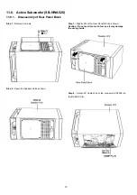
Page 70: ...el Block Step 1 Remove 6 screws Step 2 Upset the Speaker Unit as shown Step 3 Slightly lift out the Rear Panel Block as shown Caution Do not exert too much force as it may damage the wiring inside Step 4 Detach 3P Cable Wire of the connector CN1003 on the DAMP P C B ...

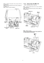
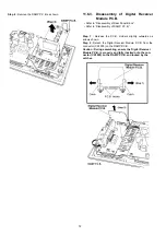
Page 71: ...ove the Rear Panel Block 11 6 2 Disassembly of DAMP P C B Refer to Disassembly of Rear Panel Block Step 1 Detach 4P Cable Wire from the connector CN1002 on the DAMP P C B Step 2 Detach 7P Cable Wire from the connector CN201 on the SMPS P C B Step 3 Remove 4 screws Caution During assembling ensure that the DAMP P C B is seated properly onto the locators ...

Page 72: ...ssembly of DAMP P C B Step 1 Release the P C B Holders slightly outwards as arrows shown Step 2 Detach the Digital Receiver Module P C B from the connector CN1000 on the DAMP P C B Caution During assembling ensure the Digital Receiver Module P C B is properly and fully inserted onto the con nector CN1000 on the DAMP P C B and locked by the catches ...

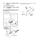
Page 73: ... of DAMP P C B 11 6 4 1 Disassembly of Digital Amplifier IC IC5200 Caution Avoid touching the DAMP Heatsink P C B due to its high temperature after prolonged use Touching is may lead to injuries Step 1 Remove Heatsink Clip Step 2 Desolder the pins of Digital Amplifier IC IC5200 on the solder side of the DAMP P C B ...

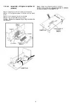
Page 74: ...lifier IC IC5200 onto the DAMP P C B Step 3 Fix the Heatsink Clip onto the Heatsink Step 4 Flip over the DAMP P C B as shown Caution Ensure the Heatsink Clip is fully inserted onto the Heatsink Step 5 Solder pins of Digital Amplifier IC IC5200 Caution Ensure the pins of Digital Amplifier IC IC5200 are properly seated on the DAMP P C B ...

Page 75: ...rrow shown Caution During assembling ensure that the Power Button P C B is seated properly onto the locators 11 6 6 Disassembly of SMPS Module P C B Refer to Disassembly of Rear Panel Block Step 1 Detach 7P Cable Wire at the connector CN201 on the SMPS Module P C B Step 2 Remove 4 screws Caution During assembling ensure that the SMPS Mod ule P C B is seated properly onto the locators ...

Page 76: ...76 Step 3 Remove the SMPS Module P C B as arrow shown 11 6 7 Disassembly of Bottom Panel Block Step 1 Remove 4 screws Step 2 Remove the Bottom Panel Block as shown ...

Page 77: ...ough the hole of the Speaker Unit as shown Caution During assembling ensure that the 2P Cable Wire is properly inserted through the hole of Speaker Box as diagram shown Caution During assembling ensure the locators of the AC Inlet Unit are properly inserted into the guides as diagram shown Step 3 Remove 1 screw Step 4 Remove the AC Inlet P C B from the AC Cover as arrow shown ...

Page 78: ...ed into the slots of AC Cover as diagram shown 11 6 9 Disassembly of Woofer Speaker SP61 Refer to Disassembly of Bottom Panel Step 1 Remove 4 screws Step 2 Lift up to remove Woofer Speaker SP61 Step 3 Detach the Red wire and Black wires Step 4 Remove the Woofer Speaker SP61 ...

Page 79: ...diagram shown 12 1 2 Checking and Repairing of Main P C B Side B Step 1 Remove Top Cabinet Step 2 Remove Main P C B Step 3 Remove Front Panel Block Step 4 Attach 2P Cable Wire at the connector CN2206 on Main P C B Step 5 Attach 40P FFC at the connector CN2201 on Main P C B Step 6 Attach 17P FFC at the connector CN2205 on Main P C B Step 7 Attach 11P FFC at the connector CN2204 on Main P C B Step 8...

Page 80: ... 12 1 3 Checking and Repairing of SMPS P C B Step 1 Remove Top Cabinet Step 2 Remove SMPS P C B Step 3 Attach 9P FFC at the connector CN1 on SMPS P C B Step 4 Attach 6P Cable Wire at the connector CN5900 on DAMP P C B Step 5 Upset SMPS P C B as arrow shown Step 6 Place the SMPS P C B on an Insulated Material Step 7 SMPS P C B can be checked and repaired as diagram shown ...

Page 81: ...s arrow shown Caution 1 Keep the Heatsink Spacer in safe place Avoid denting it place it back during assembling Caution 2 Handle the DAMP Heatsink P C B with caution due to it s high temperature after prolonged use Touching it may lead to injuries Step 7 Attach 6P Cable Wire at the connector CN5900 on DAMP P C B Step 8 Attach 40P FFC at the connector CN5200 on DAMP P C B Step 9 DAMP P C B A side c...

Page 82: ...TB15 from the connector CN2201 on the Main P C B to the connector CN5200 on DAMP P C B Step 8 DAMP P C B B side can be checked and repaired as diagram shown 12 1 6 Checking and Repairing of Panel P C B Step 1 Remove Top Cabinet Step 2 Remove Front Panel Block Step 3 Remove Button P C B and Panel P C B Step 4 Attach 2P Cable Wire at the connector CN2206 on Main P C B Step 5 Attach 17P FFC at the co...

Page 83: ...n the SMPS Module P C B Step 5 Attach 7P Cable Wire at the connector CN201 on the SMPS Module P C B Step 6 Attach 4P Cable Wire at the connector CN1002 on the DAMP P C B Step 7 Attach 3P Cable Wire at the connector CN1003 on the DAMP P C B Step 8 Attach 2P Extension Cable REXX1194 from the Speaker Cable and the connector CN1005 on the DAMP P C B Step 9 Lift and upset the SMPS Module P C B AC Inlet...

Page 84: ...84 ...

Page 85: ...nlet ECO_CON BK5V PVCC 28 5V 20V HDMI IN 2 TMDS HPO DDC Jitter IC HDMI_3 3V 5V Power 5V Power LDO 5V Power Video Data Q0 Q31 SPDIF SPDIF OPT IN 2 SPDIF SPDIF ARC PWM_FL PWM_FR DC DET CCT ECO_Level CCT DC_DET ECO LEVEL OTW SD A0 A9 DQ0 DQ15 DSP_SCLK DSP_LRCLK DSP_SD1 Valid DAP_I2C 2 IN 1 OUT ADC ADC_MS SL ADC_PDN ADC_MS SL ADC_PDN OMCK 2 IN 1 GP00 GP01 WL_DSP_SD2 WL_DSP_SD3 WL_DSP_SCLK WL_DSP_LRCLK...

Page 86: ...r 16M SDRAM IC2003 CODEC IC2401 DSP IC2001 Damp IC5300 Opt 1 Opt 2 LDO IC2902 Op Amp IC2101 ADC IC2102 Bluetooth Wireless Panel LED X 8 EEPROM Micro P IC2301 Driver IC6001 Remote DC_DC Con IC2803 DC_DC Con IC2804 LDO IC2802 DC_DC Con IC5801 2 35A ADC IC2102 Analogy SW IC2104 IC2303 ROHM Jitter Free IC5301 IC2103 REG10V 34mA HDMI Pcon Po A m 0 4 4 V 8 1 I M D H W 7 1 0 Pd 0 51 W 5mA 350mA 150mA Po ...

Page 87: ...DC DET 86 DATA 2 CLK 3 LCK 4 OE 17 DC DET DC DET W INT 87 W INT W INT W SDI 98 W SDI W SDI W DET 64 W DET W DET ECO LVL 91 ECO LEVEL ECO LEVEL RX INT 42 RX INT RX INT TX INT 41 TX INT TX INT TX HPD 66 TX HPD TX HPD VSYNC COUNT 4 VSYNC VSYNC RX0 5V DET 56 RX0 5V RX0 5V RX1 5V DET 55 5V DET 65 RX1 5V RX1 5V S DET 93 S DET PCONT 88 MUTE ALL 22 RESET CODEC 67 CS CODEC CS CODEC CS CODEC 58 CLK DSP 77 M...

Page 88: ... 12 DAI DAT0 DAI DAT0 DAI DAT1 DAI DAT1 DAI DAT2 DAI DAT2 DAI DAT3 DAI DAT3 SPDIF SPDIF 2Y1 9 2Y2 7 2Y3 5 2Y4 3 Q2508 CEC INTERFACE HDMI SWITCHING CIRCUIT Q2503 HOTPLUG SWITCH 3 3V 5V DE 19 DE 1 HSYNC 20 HSYNC 2 VSYNC 21 VSYNC 3 1OE 1 2OE 19 TO AUDIO FROM TO SYSTEM CONTROL FROM TO SYSTEM CONTROL FROM TO SYSTEM CONTROL HDMI AV IN AUX1 HDMI2 JK2701 EEPROM C3EBEY000042 QR2701 QR2702 Q2701 Q2702 Q2703...

Page 89: ...CN5200 CN2201 VALID DAP SCL DAP RESET DAP MUTE 18 23 CN5200 CN2201 DC DET DC DET 12 29 CN5200 CN2201 ECO LEVEL ECO LEVEL ECO LEVEL 8 33 CN5200 CN2201 SD SDI SCL SSB WCLK BCLK ADAT0 AGND INT SDO SD 9 32 CN5200 CN2201 PWM A PWM B PWM C PWM D RST AB L RST CD L DIGITAL AMPLIFIER C1AB00003217 IC5300 5 SD L OTW OTW 10 31 CN5200 CN2201 2 OTW L 6 8 16 18 7 17 OUT A 39 BST A 43 OUT B 36 BST B 34 OUT D 28 B...

Page 90: ...1 4 R1X1 66 TMDS D2 3 R1X2 69 TMDS D2 1 R1X2 R1X0 R1X0 R1X1 R1X1 R1X2 R1X2 70 IC2601 HDMI RECEIVER SIGNAL NAME TC 2 PIN NO PORT NAME PIN NO PORT NAME EXT A0 102 A0 21 EXT A1 101 A1 22 EXT A2 99 A2 23 EXT A3 97 A3 24 EXT A4 96 A4 27 EXT A5 93 A5 28 EXT A6 91 A6 29 EXT A7 90 A7 30 EXT A8 88 A8 31 EXT A9 87 A9 32 EXT A10 103 A10 A0 A1 A2 A3 A4 A5 A6 A7 A8 A9 A10 20 IC2003 16M SDRAM IC2001 DSP SIGNAL ...

Page 91: ...T S DET 30 11 CN2201 CN5200 REG12V REG12V 3 4 5 36 37 38 CN2201 CN5200 DC20V DC20V 1 1 CN5900 JW1 PVCC PVCC 3 4 3 4 CN5900 JW1 DC20V DC20V 1 2 8 9 CN2202 CN1 BK5V BK5V BK 3 3V 3 VIN 5 CE 3 3V VOLTAGE REGULATOR C0DBEYY00146 IC2802 VOUT 1 ADJ 4 BK5V BK5V 5 5 CN2202 CN1 DC DET DC DET 8 2 CN2202 CN1 SYNC SYNC SYNC SYNC 9 1 CN2202 CN1 PCONT DAMP PCONT DAMP 25 16 CN2201 CN5200 REG3 3V REG3 3V 34 35 6 7 ...

Page 92: ...G3 3V REG3 3V D2326 REG3 3V VOUT 2 ADJ 4 REG12V 1 VIN 3 3V VOLTAGE REGULATOR C0DBAYH00005 IC2803 REG5V VOUT 2 ADJ 4 REG12V 1 VIN 5V VOLTAGE REGULATOR C0DBAYH00005 IC2804 QR2312 DC DETECT D2325 D2322 D2323 D2324 5V 5V RF 5V 5V 13 14 4 5 CN3001 CN2205 17 17 CN3000 MAIN P C B VREF 3 3V VREF 3 3V VREF 3 3V 3 3V REG5V REG5V 5V 2 10 CN6001 CN2204 REG5V 11 1 CN6001 CN2204 PANEL P C B REG12V S DET REG3 3V...

Page 93: ...1004 MODE SW 1 4 CN1002 H1004 PCONT 7 7 CN1000 RF MUTE 10 10 CN1000 LINK LED CH2 R OUT IDSET DC DET 5V RF PCONT RF MUTE LINK 8 8 CN1000 5V PCONT 23V 23V MUTE 5V 7 7 H1001 CN201 P5701 POWER AMPLIFIER C1BA00000497 IC5200 Q1007 Q1008 SPEAKER PROTECTION SWITCH OUT1 10 BOOT1 9 OUT2 14 BOOT2 15 3 IN1 22 IN2 23 MODE 2 CN1005 1 CN1005 2 1 6 7 DUAL OP AMP C0ABBB000244 IC3002 23 5V 16V Q2002 16V VOLTAGE REG...

Page 94: ...0 CN3001 CN6001 21 1 22 2 1 17 11 1 10 2 2 16 C PANEL P C B SOLDER SIDE JW6002 3 1 B DAMP P C B Side B SOLDER SIDE G SMPS P C B SOLDER SIDE 1 6 1 40 1 6 1 9 2 8 A MAIN P C B Side B SOLDER SIDE 2 1 1 11 1 6 2 10 1 9 2 10 1 17 2 16 9 1 8 2 1 40 CAUTION RISK OF ELECTRIC SHOCK AC VOLTAGE LINE PLEASE DO NOT TOUCH THIS P C B 110V 240V 50 60Hz GS GSX 220V 50Hz GK JW1 P5701 T5701 CN1 MAIN TRANSFORMER AC I...

Page 95: ... MODULE P C B RED BLK AC IN TO DIGITAL RECEIVER MODULE TO LED P C B TO SUBWOOFER J AC INLET P C B SOLDER SIDE I POWER BUTTON P C B SOLDER SIDE H DAMP P C B SOLDER SIDE 1 4 1 4 7 1 22 2 21 1 1 3 TO SMPS MODULE P C B SC HTB550GK GS GSX SB HWA520GK GS GSX WIRING CONNECTION DIAGRAM 110V 240V 50 60Hz GS GSX 220V 50Hz GK ...

Page 96: ...96 ...

Page 97: ...s shown in the parts list In case of AC rated voltage Capacitors the part no and val ues will be indicated in the Schematic Diagram AC rated voltage capacitors C5700 C5701 C5702 C5703 C5705 Resistor Unit of resistance is OHM Ω K 1 000 M 1 000 000 Capacitor Unit of capacitance is μF unless otherwise noted F Farads pF pico Farad Coil Unit of inductance is H unless otherwise noted REF IS FOR INDICATI...

Page 98: ...98 ...

Page 99: ...2 C0JBAB000986 DUAL INVERTER LB2505 J0JHC0000078 G3 G4 G1 G2 5 3 4 7 9 8 6 1 2 10 13 15 17 19 18 16 14 11 12 JK2501 6 8 7 5 2 1 4 3 L2502 J0ZZB0000148 3 1 2 4 5 IC2503 C0CBCDD00004 5V VOLTAGE REGULATOR VA2509 R2517 220 C2510 0 1 R2508 27K R2509 1K 3 1 2 4 5 Q2508 B1CFGD000002 CEC INTERFACE DDC CEC GND 5V POWER HOT PLUG CLK GND TMDS D0 TMDS CLK DDC_SCL HEAC ARC DDC_SDA CEC TMDS CLK TMDS D2 TMDS D2 ...

Page 100: ... 81 82 80 86 87 88 84 83 85 45 19 17 15 14 16 18 43 23 21 20 22 41 24 39 37 33 32 31 30 29 28 27 26 36 35 34 38 25 40 42 44 13 46 IC2501 C1AB00002975 HDMI TRANSMITTER C2534 10 CEC_IO R2540 4 7K C2523 10 LB2509 LB2509 LB2512 J0JHC0000078 LB2512 LB2511 LB2510 D21 D22 D19 D20 D25 D23 D24 C2520 R2539 D35 D32 D33 D29 D28 D30 D26 D27 D31 D34 C2522 C2529 1000P 1000P C2525 C2535 C2521 C2524 0 1 0 1 C2532 ...

Page 101: ...2 3 1 5 4 6 Q2601 R2615 10K R2611 QR2702 QR2701 C2705 1 RX01_EDID_DT R2606 47K 47K R2613 10K RX0_HPD Q2605 RX1_HPD 2 3 1 5 4 6 Q2603 VA2611 R2614 100 R2714 100 VA2711 R2710 47K R2610 47K VA2612 RX0_5V 15K R2721 82K R2722 RX0_WRT_SEL RX01_EDID_CK 2 1 7 4 3 6 5 8 IC2603 C3EBEY000042 EEPROM RX1_5V 15K R2621 QR2701 QR2702 B1GBCFJJ0048 HOTPLUG DETECT QR2601 QR2602 B1GBCFJJ0048 HOTPLUG DETECT R2718 1K V...

Page 102: ...RX2611 C2627 D5 D4 8 6 5 7 4 2 1 3 RX2603 C2635 1000P LB2608 LB2607 LB2607 LB2608 J0JHC0000078 R2646 4 7K D3 8 6 5 7 4 2 1 3 RX2602 C2632 C2633 1 1 C2634 95 94 98 99 96 97 92 91 93 106 107 102 103 100 101 105 104 108 109 T1 114 130 144 140 141 135 137 136 132 133 131 134 139 138 143 142 118 121 119 120 116 115 117 128 129 124 125 122 123 127 126 112 110 111 113 52 53 54 55 56 57 58 59 60 61 62 63 ...

Page 103: ...8 57 52 51 54 53 65 66 61 62 59 60 64 63 70 69 73 75 10 8 7 9 12 11 99 100 95 94 96 97 90 91 89 93 92 98 4 6 5 2 1 3 81 82 80 86 87 88 84 83 85 45 19 17 15 14 16 18 43 23 21 20 22 41 24 39 37 34 35 33 32 27 31 30 29 28 26 36 38 25 40 42 44 13 46 IC2301 RFKWMHTB550P MICROPROCESSOR RX01_EDID_DT BK_3 3V GND CEC_IO S_DET S_DET R2310 100K 150K R2307 R2312 1K 3 1 2 X2301 VSYNC_M DP DP DP DP DP OPT GND C...

Page 104: ... RXD EPM GND GND VCC SLCK BUSY MON_RESET RESET RESET CNVSS CNVSS MON_SW SYNC ECO_CONT BK_5V HTB550 GS GSX GK GS GSX GK GND CE VOUT ADJ VIN HTB550 MUTE_ALL AC_SYNC VIN DP ADJ GND VOUT ON OFF VIN ADJ GND VOUT ON OFF GND DC20V DC20V GND SW_STOP SMPSDET R2817 0 G4 C2853 1000P LED_LCK KEY2 LED_CLK VREF 3 3V VREF GND REG5V DGND KEY1 REMOTE LED_OE LED_DATA CN2204 LB2864 LB2865 LB2867 LB2866 LB2863 LB2862...

Page 105: ...7 1000P C2444 0 022 C2412 0 1 C2409 C2442 10 0 1 C2401 0 1 C2443 R2418 100 CLK_DSP MOSI_DSP DT_OUT_CODEC R2419 100 INTREQ_CODEC 1K R2422 1K R2417 0 01 C2420 C2428 0 01 C2429 0 01 1K R2415 ARC 1000P C2425 100P C2403 100P C2422 6 3V100 C2440 47K R2420 C2423 100P CS_CODEC RESET_CODEC R2008 33 C2405 0 01 R2411 47K C2411 0 01 6 3V100 C2406 C2413 0 01 12 13 11 10 2 3 1 7 8 9 5 4 6 16 18 20 22 25 23 24 2...

Page 106: ...CODEC CS_CODEC CLK_DSP 0 1 C2014 0 1 C2017 0 1 C2015 103 107 106 110 113 119 118 124 127 128 125 126 121 120 123 122 115 114 117 116 111 112 108 109 104 105 61 62 12 11 14 15 13 18 19 16 17 9 5 7 6 3 1 2 4 8 10 57 26 28 29 27 22 21 24 25 23 45 46 47 42 43 40 39 41 44 37 38 34 33 35 31 30 32 36 55 56 51 52 49 48 50 54 53 20 58 59 60 63 64 95 94 100 99 102 101 96 98 97 85 84 87 86 83 80 81 76 68 69 ...

Page 107: ...P_GND DAP_SDA DSP_GND DSP_SCLK DSP_MCLK FAN_DA DAP_PDN DAP_RESET PCONT_INV DSP_LRCLK DSP_SD3 C SW DSP_SD2 SL SR DSP_SD1 FL FR DC_DET DSP IRQ DSP CLIP DSP MODE OPT_GND OPT_GND OPT_GND OPT1_IN OPT2_IN REG3 3V VCC OUTPUT GND OUTPUT REG3 3V VOUT VIN ADJ GND ON OFF R5351 2 2 R5350 0 PWM_FL PWM_FL PWM_FR PWM_FR C5352 1000P C5332 1000P C5372 10 C5371 1000P 10 C5331 C5351 10 R5324 22 R5364 0 C5219 0 1 DAP...

Page 108: ...100H00018 C5418 0 01 C5423 1000P C5424 1000P R5412 R5420 0 0 R5406 3 3 C5414 0 1 C5420 1 C5101 0 1 C5103 0 1 R5401 10 R5104 100 G1 G2 2 1 4 3 P5100 IC5300 C1AB00003217 DIGITAL AMPLIFIER VALID PWM_FL PWM_FL 47 R5417 R5416 47 PWM_FR PWM_FR OTW R5317 47 R5316 47 SD R5105 10 C5102 10 D5803 R5817 47K C5804 1 L5901 J0JKB0000020 2 4 3 1 6 5 CN5900 L5902 J0JKB0000020 39K R5818 C5802 10 R5806 33K R5811 100...

Page 109: ...180 R6004 220 R6013 180 R6003 180 R6009 220 1 3 2 JW6002 D6002 B3ABA0000187 D6003 B3ABA0000187 D6006 B3ABA0000187 D6004 B3ADA0000087 D6007 B3ABA0000187 R6001 180 D6001 B3ABA0000187 R6010 100 Q0 DATA Q3 Q4 Q1 Q2 CLK LCK GND OE Q7 Q5 Q6 Q9 Q8 Q11 Q10 VDD GS GSX GK KEY1 KEY2 VREF GND LED_OE DGND REG5V KEY1 KEY2 REMOTE VREF 3 3V LED_CLK LED_DATA LED_LCK VREF GND RE VDD GND S6003 1 2K 1 2K R6006 1 3 2 ...

Page 110: ...6 5 JW1 C5805 35V470 B0BC020A0267 D5704 R5702 100K D5702 B0EAKT000063 C5713 0 01 R5703 100K 470K R5760 10K R5762 10K R5763 Q5761 B1ABCN000001 OP AMP C5761 0 1 Q5760 B1ADCN000010 CURRENT LIMITING SWITCH C5726 50V10 DCDET SYNC 3 2 1 ZJ5703 33K R5766 R5818 2 2K C5820 56P C5819 56P A R K R5802 3 3K 6800P C5817 R5814 1K R5810 220 R5806 10K 100K R5861 C5869 0 01 R5804 100K R5728 22K C5828 6 3V470 R5819 ...

Page 111: ...4 7 2 1 4 3 22 21 CN1000 D1000 0 C4000 0 1 5V 23 5V R1003 0 0 R1034 1 3 2 CN1003 4 5 1 3 2 7 6 H1001 DC_DET MODE_SW RF_MUTE 1K R1020 10K R5770 B1GBCFJJ0051 VOLTAGE SUPPLY CONTROL Q1009 PGND PCONT 23 5V 5V GND 23 5V 5V 5V DC_DET LINK_LED 5V_GND NC NC DGND RF_MUTE NC NC NC NC NC DC_DET 5V AGND AGND IDSET MODE_SW POWER_SW 5V_GND 5V_GND CH2_IN_LCH CH2_IN_RCH IDSET PCONT LINK_LED NC LED2 LED1 Z1000 3 2...

Page 112: ...4 0 1 R5208 5 6K R5207 5 6K C5216 330P C5215 0 1 C5233 0 47 C5232 0 47 C5204 0 015 C5220 0 1 R5201 10 220P C5218 0 1 C5219 220P C5205 C5234 1000P C5209 0 1 R5200 10 220P C5211 R5206 5 6K R5205 5 6K C5208 0 1 C5210 0 1 C5200 0 1 C5212 220P C5201 0 015 R1015 33K 330P C5224 C1004 25V1000 C1002 0 1 220P C5203 C5222 0 47 C5223 0 47 C5522 R5210 10 0 1 C5207 0 1 C5213 1000P C5221 1000P C5231 C5602 16V10 ...

Page 113: ... 60Hz GS GSX 220V 50Hz GK I POWER BUTTON CIRCUIT SCHEMATIC DIAGRAM 15 J AC INLET CIRCUIT H TO DAMP CIRCUIT CN1002 IN SCHEMATIC DIAGRAM 13 TO SMPS MODULE NOTE REF IS FOR INDICATION ONLY SC HTB550GK GS GSX SB HWA520GK GS GSX POWER BUTTON AC INLET CIRCUIT P5701 TL10 TL20 RED BLK I D SET S1000 2 1 1 4 4 3 H1004 6 3 4 1 S1001 POWER IDSET MODE_SW POWER_SW 5V_GND ...

Page 114: ...01 VA2510 VA2513 VA2511 VA2512 IC2603 IC2703 QR2701 QR2702 Q2703 Q2704 Q2702 Q2701 R2710 R2712 R2718 R2714 R2709 R2708 R2707 R2717 R2716 R2715 R2719 R2720 R2713 R2915 C2706 C2705 VA2710 VA2709 VA2711 VA2712 LB2704 LB2706 LB2703 LB2705 C2605 QR2601 QR2602 Q2606 Q2605 Q2602 Q2601 R2607 R2606 R2611 R2614 R2618 R2609 R2604 R2608 Q2603 Q2604 LB2604 LB2606 LB2603 LB2605 R2610 R2612 VA2610 VA2609 VA2611 ...

Page 115: ...8 R2598 R2592 R2589 R2583 R2585 R2587 IC2501 C2551 C2532 C2531 C2530 R2647 LB2610 R2551 R2546 R2545 RX2501 C2526 R2542 R2544 R2543 R2538 L2502 L2501 R2540 R2536 R2537 R2539 IC2601 RX2604 RX2601 RX2602 RX2603 R2735 R2734 R2636 R2637 R2634 R2635 R2721 R2722 R2711 R2706 R2704 Q2705 Q2706 R2605 C2604 JK2701 JK2601 JK2501 R2643 R2645 RX2611 R2641 R2646 R2638 LB2609 R2642 X2601 R2644 C2638 C2631 C2630 R...

Page 116: ...5 R5301 C5372 R5364 X5302 D5801 R5206 C5331 R5805 L5401 R5102 C2926 R5359 D5301 R5203 HEATSINK R5402 R5802 C5309 R5417 R5351 C5381 C5202 R5385 D5905 C5409 C5346 C5375 R5366 C5802 R5407 IC5301 L5901 C5343 R5316 R5104 C5371 R5363 R5922 L5405 C5319 R5205 R5804 L5305 R5101 L5905 R5358 C5925 R5202 C5419 C5220 C5380 R5401 R5801 C5308 RL5005 R5416 C5923 R5350 P5100 D5805 C5320 C5402 C5408 D5802 C5373 R53...

Page 117: ...012 R6011 C6011 C6010 R6012 R6014 R6015 R6013 R6004 R6009 R6003 R6002 R6001 C6008 W1 W2 W3 W4 C6002 JW6002 CN6001 D6001 D6007 D6004 D6006 D6003 D6002 Z6001 R6006 R6007 JW6003 S6002 S6003 S6004 LB3001 LB3004 LB3006 R3004 R3005 R3006 R3008 R3009 R3010 R3013 R3014 W3002 W3001 LB3014 R3002 R3003 LB3013 R3001 C3001 C3000 R3007 W3003 CN3000 CN3001 ET3000 C3003 JW6004 S6001 VOL DOWN VOL UP SELECTOR POWER...

Page 118: ...2 R5760 Q5760 D5760 C5761 R5867 D5812 R5823 C5700 C5702 C5703 C5705 C5712 C5726 C5727 C5747 C5814 D5701 D5712 DZ5701 IC5701 JW1 K102 K103 K104 L5703 L5702 Q5720 R5727 T5701 TH5702 ZJ5701 ZJ5703 W3 W2 IC5801 C5828 W11 W10 W6 D5802 W5 W13 C5805 W14 K5701 K101 W17 W18 F1 CN1 D5803 D5721 MAIN TRANSFORMER T3 15A 250V C5701 C5713 C5791 C5808 D5702 GS GSX GK K5726 HTB550 QR5862 R5702 R5703 R5862 R5864 ZA...

Page 119: ...06 W1003 R1000 Q1008 Q1009 R1020 W1031 C5603 R2010 R2000 C1003 C3105 R1034 R5769 W1052 C4000 R1003 R1015 C1012 R3204 R3206 R1207 C3205 R1107 R5770 K1004 L1006 C5207 C5213 L1005 R3212 R3211 R3114 R3113 W1055 D1000 W1057 C1010 Q1007 W1018 W1021 L1003 L1004 Q2002 HEATSINK Q2010 C1014 C2010 C5602 W1017 W1008 W1007 W1009 W1014 C2001 W1011 W1020 W1013 W1022 W1010 K1003 W1012 W1027 W1028 Q1003 CN1003 W10...

Page 120: ...120 ...

Page 121: ...3 3 3 3 3 STANDBY 0 1 8 0 1 7 0 1 7 0 0 9 0 3 4 1 7 0 0 1 7 1 8 0 3 3 3 3 3 3 3 3 REF NO MODE 61 62 63 64 65 66 67 68 69 70 71 72 73 74 75 76 77 78 79 80 HDMI 3 3 3 4 3 3 3 2 1 3 3 4 0 3 2 3 3 3 3 3 3 3 3 3 3 0 0 0 0 0 1 9 0 STANDBY 3 3 3 4 3 3 3 2 1 3 3 4 0 3 2 3 3 3 3 3 3 3 3 3 3 0 0 0 0 0 1 9 0 REF NO MODE 81 82 83 84 85 86 87 88 89 90 91 92 93 94 95 96 97 98 99 100 HDMI 3 4 0 1 8 0 0 0 0 0 0 0...

Page 122: ... 3 0 3 2 3 2 3 4 3 2 3 4 0 3 4 0 0 3 3 3 1 3 2 0 8 0 STANDBY 0 0 2 8 0 3 0 3 2 3 2 3 4 3 2 3 4 0 3 4 0 0 3 2 3 1 3 2 0 1 6 REF NO MODE 81 82 83 84 85 86 87 88 89 90 91 92 93 94 95 96 97 98 99 100 HDMI 1 6 0 0 3 2 3 2 3 1 2 9 3 1 3 2 2 9 1 6 1 8 0 0 0 3 2 3 2 0 0 0 STANDBY 1 6 0 3 2 3 2 3 1 2 9 3 1 3 1 3 2 3 2 1 6 1 8 3 1 0 0 3 3 3 2 0 0 0 REF NO MODE 1 2 3 4 5 6 7 8 POWER ON 3 2 3 2 0 0 3 2 3 2 0 ...

Page 123: ... 5 6 POWER ON 1 6 0 1 3 3 1 3 3 1 7 STANDBY 1 6 0 1 3 3 1 3 3 1 7 REF NO MODE 1 2 3 4 5 POWER ON 3 1 0 1 3 5 6 0 STANDBY 3 1 0 1 3 5 6 0 REF NO MODE 1 2 3 4 5 6 7 8 9 10 11 12 13 14 15 16 17 18 19 20 POWER ON 1 6 1 6 1 6 0 1 7 3 4 1 7 1 7 1 7 1 7 0 1 8 1 7 1 7 1 7 1 7 0 3 4 2 6 3 2 STANDBY 1 6 1 6 1 6 0 1 7 3 4 1 7 1 7 1 7 1 7 0 1 8 1 7 1 7 1 7 1 7 0 3 4 2 6 3 2 REF NO MODE 21 22 23 24 25 26 27 28...

Page 124: ... 0 0 0 3 3 0 0 0 0 0 1 8 0 1 1 1 1 0 8 0 3 4 0 0 0 REF NO MODE 141 142 143 144 POWER ON 0 0 0 0 STANDBY 0 0 0 0 REF NO MODE 1 2 3 4 5 6 7 8 9 10 11 12 13 14 15 16 17 18 19 20 POWER ON 1 0 1 7 1 7 1 7 0 1 7 0 0 2 0 0 0 0 2 0 1 7 0 1 7 1 7 1 7 1 0 3 3 STANDBY 1 0 1 7 1 7 1 7 0 1 7 0 0 0 0 0 0 0 1 7 0 1 7 1 7 1 7 1 0 3 3 REF NO MODE 1 2 3 4 5 6 7 8 POWER ON 0 0 0 0 5 0 5 0 3 3 5 0 STANDBY 0 0 0 0 5 0...

Page 125: ... 0 3 0 3 0 3 2 3 0 3 0 0 3 2 3 2 3 2 REF NO MODE 1 2 3 4 5 1 2 3 4 5 E C B E C B HDMI 1 2 0 1 2 0 5 0 1 2 0 1 2 5 0 3 2 0 5 0 3 1 0 5 0 3 1 STANDBY 1 2 0 1 2 0 5 0 1 2 0 1 2 5 0 3 2 0 5 0 3 1 0 5 0 3 1 REF NO MODE E C B E C B HDMI 0 4 9 0 0 5 0 0 STANDBY 0 4 9 0 0 5 0 0 REF NO MODE 1 2 3 4 5 1 2 3 4 5 1 2 3 4 5 6 POWER ON 3 0 0 3 2 3 2 3 2 3 0 0 3 2 3 2 3 2 5 0 0 0 4 7 5 0 4 6 STANDBY 3 0 0 3 2 3 ...

Page 126: ... 2 0 0 3 2 3 2 0 3 2 STANDBY 0 3 1 0 0 3 1 0 0 0 3 2 0 0 3 2 3 2 0 3 2 REF NO MODE E C B E C B E C B E C B POWER ON 0 0 3 3 0 0 13 5 0 0 3 2 0 2 0 0 STANDBY 0 0 3 3 0 0 13 5 0 0 3 2 0 2 0 0 QR2304 QR2303 SC HTB550GK GS GSX SU HTB550GK GS GSX MAIN P C B QR2306 QR2301 QR2305 QR2312 QR2801 QR2804 QR2302 ...

Page 127: ...ANDBY 20 5 0 21 2 12 REF NO MODE 1 2 3 4 5 6 7 8 9 10 11 12 13 14 15 16 17 18 19 20 POWER ON 0 3 3 0 0 0 0 1 5 1 7 3 3 0 0 3 2 0 1 7 3 3 0 1 5 1 5 1 5 0 STANDBY 0 3 3 0 0 0 0 1 5 1 7 3 3 0 0 3 2 0 1 7 3 3 0 1 5 1 5 1 5 0 REF NO MODE 21 22 23 24 25 26 27 28 29 30 31 32 33 34 35 36 37 38 39 40 POWER ON 1 7 1 7 1 7 0 1 1 0 0 3 3 3 3 1 7 1 7 0 0 0 0 0 3 4 3 4 3 4 1 7 STANDBY 1 7 1 7 0 0 0 0 0 3 3 3 3 ...

Page 128: ... 9 3 9 3 2 0 7 3 8 0 3 2 IC6001 SC HTB550GK GS GSX SU HTB550GK GS GSX PANEL P C B REF NO MODE 1 2 3 4 5 6 7 POWER ON 159 3 0 7 0 0 0 1 7 8 0 STANDBY 159 3 0 7 0 0 0 1 7 8 0 REF NO MODE K A R POWER ON 18 3 0 2 5 STANDBY 18 3 0 2 5 REF NO MODE 1 2 3 4 POWER ON 4 5 4 5 0 0 STANDBY 4 5 4 5 0 0 REF NO MODE E C B E C B E C B E C B E C B POWER ON 6 9 7 8 6 9 0 7 0 7 2 0 7 0 7 2 0 0 9 0 0 4 0 STANDBY 6 9 ...

Page 129: ...22 9 0 9 0 23 1 22 7 22 7 0 22 8 REF NO MODE 21 22 23 HDMI 7 7 0 4 9 STANDBY 7 7 0 4 9 REF NO MODE E C B E C B E C B E C B E C B POWER ON 5 1 5 0 4 3 4 6 4 7 0 0 0 2 9 0 4 3 3 3 0 2 5 0 STANDBY 5 1 5 0 4 3 4 6 4 7 4 2 0 0 2 9 0 4 3 3 3 0 2 5 0 REF NO MODE E C B E C B E C B E C B E C B POWER ON 0 2 6 0 0 2 8 0 15 8 22 9 16 4 0 15 7 0 6 15 1 22 7 15 5 STANDBY 0 2 6 0 0 2 8 0 15 8 22 9 16 4 0 15 7 0 ...

Page 130: ...div WF No IC2501 58 PLAY 5Vp p 5usec div WF No IC2501 56 PLAY 5Vp p 5usec div WF No IC2501 57 PLAY 5Vp p 5usec div WF No IC2001 27 PLAY 5Vp p 1usec div WF No IC2501 9 PLAY 3Vp p 500nsec div WF No IC2501 59 PLAY 5Vp p 5usec div WF No IC2501 60 PLAY 5Vp p 5usec div WF No IC2001 51 PLAY 6Vp p 1usec div WF No IC2401 10 PLAY 8Vp p 1usec div WF No IC2001 34 PLAY 4Vp p 1usec div WF No IC2001 48 PLAY 6Vp ...

Page 131: ...WF No IC2601 111 PLAY 6Vp p 5usec div WF No IC2601 115 117 PLAY 6Vp p 5usec div WF No IC2601 116 PLAY 6Vp p 5usec div WF No IC2501 71 PLAY 3Vp p 10usec div WF No IC2501 67 PLAY 1 5Vp p 5usec div WF No IC2501 68 69 PLAY 0 04Vp p 5usec div WF No IC2501 70 PLAY 0 024Vp p 5usec div WF No IC2501 72 PLAY 5Vp p 2usec div WF No IC2501 73 PLAY 5Vp p 2usec div WF No IC2501 74 75 PLAY 5Vp p 2usec div SC HTB5...

Page 132: ...01 135 PLAY 6Vp p 5usec div WF No IC2602 3 PLAY 8Vp p 500nsec div WF No IC5300 6 8 16 18 PLAY 6Vp p 1usec div WF No IC5300 28 31 36 39 PLAY 28Vp p 1usec div WF No IC5301 7 PLAY 1 25Vp p 20nsec div WF No IC5301 8 PLAY 4 4Vp p 20nsec div WF No IC5301 40 45 46 47 48 PLAY 6 4Vp p 1usec div WF No IC5301 41 PLAY 6Vp p 1usec div SC HTB550GK GS GSX SU HTB550GK GS GSX SC HTB550GK GS GSX SB HWA520GK GS GSX ...

Page 133: ...5 B1HBCFA00003 A Ca Anode Cathode B0EAKT000063 B0EAMM000057 B0HBSM000054 DZ2J033M0L DZ2J056M0L DZ2J068M0L DZ2J075M0L DZ2J150M0L DZ2J270M0L DZ2J330M0L B1BABG000007 Ca A A Ca A A 1 2 3 6 5 4 C0CBCDD00004 C0DBEYY00146 C1AB00003852 C1AB00002989 144P C0DAAYY00064 C0DAAYY00072 C3EBEY000042 1 2 3 5 4 C0EBY0000867 1 2 4 3 C2HBCY000102 128P 1 38 39 64 65 102 103 128 1 2 3 5 4 1 2 3 1 16 17 32 33 48 49 64 B...

Page 134: ...High 48 RX0 1_EDID_SCL O RX0 1 EDID ROM Serial Clock 49 RX0 1_EDID_SDA O RX0 1 EDID ROM Serial Data 50 RX1_WRT_SEL O RX1 EDID ROM write enable select Enable High 51 DSP_CLIP O PWM control 52 STBY_H O Audio output enable control Enable Low 53 RX1_HPD O Hot Plug Detect out to HDMI RX1 54 RX0_HPD O Hot Plug Detect out to HDMI RX0 55 RX1_5V_DET I Detection of connect to HDMI RX1 Detect High 56 RX0_5V_...

Page 135: ...135 99 W_SDO O Wireless control Serial Data Out 100 W_SCL O Wireless control Serial Clock Pin No Mark I O Function ...

Page 136: ...136 ...

Page 137: ...1 T5701 S6004 S6002 CN6001 S6003 S6001 P5701 P5100 DAMP HEAT SINK UNIT JW6003 JW6004 JW6002 JW1 JK5252 JK5251 JK2501 JK2701 JK2601 F1 CN5900 CN5200 CN3001 CN3000 CN2303 CN2302 CN2301 CN2206 CN2204 CN2202 CN2205 CN2201 CN1 29 28 27 26 26 26 25 24 23 22 21 21 21 21 20 20 20 19 19 19 19 19 19 19 19 18 18 18 18 18 18 18 18 18 18 18 18 17 17 16 16 15 15 15 15 15 15 13 12 1 12 11 9 8 6 4 3 2 1 a a b b c...

Page 138: ...A10 A12 1 A12 1 A12 1 A12 1 A12 1 A12 1 A12 1 A12 1 A12 A12 A11 1 A11 1 15 14 12 11 10 9 9 9 1 FRONT SPEAKER UNIT L 1 FRONT SPEAKER UNIT L R 1 FRONT SPEAKER UNIT R 1 2 3 4 5 6 7 8 9 A B C D E F G H 10 11 12 13 BAR POSITION STANDING POSITION FRONT SPEAKER UNIT L R SB HTB550GKK SB HTB550P K CABINET DRAWINGS ...

Page 139: ...EW REAR VIEW 13 13 9 9 9 9 9 9 9 9 9 9 9 9 9 9 9 9 9 9 9 9 9 9 8 7 6 5 4 3 2 3 1 3 2 a b a b f f e e c d d c FRONT SPEAKER UNIT L R 1 2 3 4 5 6 7 8 9 A B C D E F G H 10 11 12 13 SB HTB550GKK SB HTB550P K CABINET DRAWINGS ...

Page 140: ...1000 CN1005 CN1002 CN1003 CN1000 P5701 79 79 79 79 79 79 79 79 78 77 75 2 75 2 75 2 75 2 75 2 75 2 75 74 74 73 73 73 73 73 72 72 72 72 72 71 70 69 68 H1001 67 66 65 64 64 64 64 64 64 64 64 64 64 64 64 64 64 64 64 63 63 62 61 g a a b b c c d d e f f e g 1 2 3 4 5 6 7 8 9 A B C D E F G H 10 11 12 13 NOTE REF IS FOR INDICATION ONLY SB HWA520GK1 SB HWA520GS1 CABINET DRAWINGS ...

Page 141: ...HOOK A9 A8 A8 A6 A6 A5 1 A5 A4 1 A4 A3 OI BOOK A2 AC CORD FOR GK ONLY A2 AC CORD FOR GS GSX ONLY 2P FOR THAI A2 AC CORD FOR GS GSX ONLY 2P FOR EUROPEAN A2 AC CORD FOR GS GSX ONLY A1 1 R C BATTERY COVER A1 REMOTE CONTROL A12 A12 1 2 3 4 5 6 7 8 9 A B C D E F G H 10 11 12 13 P6 POLYFOAM TOP POLYFOAM BOTTOM P2 POLYFOAM LEFT POLYFOAM RIGHT P4 POLYFOAM TOP POLYFOAM BOTTOM SC HTB550GKK SC HTB550GSK SC H...

Page 142: ...142 ...
Page 143: ...EW 12 19 RHD30172 SCREW 8 20 RHDX261002 SCREW 3 21 RKA0253 H LEG CUSHION 4 22 RMCX1008 WIRELESS GROUND SPRING 1 23 RMK0804 BOTTOM CHASSIS 1 24 RMQ2001 1 TRANSMITTER HOLDER 1 25 RMQ2003 1 VOLUME BUTTON BRACKET 1 26 RMZ1105 1 HEAT SINK SPACER 3 27 RMZ1264 SMPS INSULATOR BOTTOM 1 28 RFKKUHTB350P TOP PANEL ASS Y 1 29 RSCX1060 RADIATOR SHEET 1 Safety Ref No Part No Part Name Description QTY Remarks CAB...

Page 144: ... Part No Part Name Description QTY Remarks Safety Ref No Part No Part Name Description QTY Remarks PACKING MATERIALS P1 RPG9865 PACKING CASE 1 GS GSX P1 RPG9867 PACKING CASE 1 GK P2 RPN2404 1 POLYFOAM SU HTB 1 P3 RPF0610 BAG MIRAMAT SHEET 1 P4 RPN2406 1 POLYFOAM SB HWA 1 P5 RPF0588 MIRAMAT BAG SB HWA 1 P6 RPN2405 POLYFOAM SB HTB 1 P7 RPF0578 MIRAMAT BAG SB HTB 2 P8 RPF0579 MIRAMAT BAG STAND BASE 2...

Page 145: ...003 C3ABMY000029 IC 1 IC2301 RFKWMHTB550P IC 1 IC2303 C3EBEY000042 IC 1 IC2401 C1AB00003174 IC 1 IC2501 C1AB00002975 IC 1 IC2502 C0JBAB000986 IC 1 IC2503 C0CBCDD00004 IC 1 IC2601 C1AB00002989 IC 1 IC2602 C0JBAZ001466 IC 1 IC2603 C3EBEY000042 IC 1 IC2703 C3EBEY000042 IC 1 IC2801 C0DBAYH00005 IC 1 IC2802 C0DBEYY00146 IC 1 IC2803 C0DBAYH00005 IC 1 IC2804 C0DBAYH00005 IC 1 IC2805 C0DBAYH00005 IC 1 IC2...

Page 146: ...67 DIODE 1 D5705 B0BC020A0267 DIODE 1 D5706 DA2J10100L DIODE 1 D5710 DA2J10100L DIODE 1 D5712 B0EAMM000057 DIODE 1 D5713 DZ2J330M0L DIODE 1 D5721 B0EAMM000057 DIODE 1 Safety Ref No Part No Part Name Description QTY Remarks D5760 DA2J10100L DIODE 1 D5801 DA2J10100L DIODE 1 D5802 B0HBSM000054 DIODE 1 D5802 DZ2J330M0L DIODE 1 D5803 B0EAMM000057 DIODE 1 D5803 DA2J10100L DIODE 1 D5804 DA2J10100L DIODE ...

Page 147: ...14 INDUCTOR 1 LB2869 J0JBC0000014 INDUCTOR 1 LB2871 J0JBC0000014 INDUCTOR 1 LB2872 J0JHC0000078 INDUCTOR 1 LB2874 J0JHC0000078 INDUCTOR 1 LB2876 J0JBC0000014 INDUCTOR 1 LB2877 J0JBC0000014 INDUCTOR 1 LB2878 J0JBC0000014 INDUCTOR 1 LB2879 J0JBC0000014 INDUCTOR 1 LB2880 J0JBC0000014 INDUCTOR 1 LB2881 J0JBC0000014 INDUCTOR 1 LB2883 J0JBC0000014 INDUCTOR 1 LB2885 J0JBC0000014 INDUCTOR 1 LB2886 J0JBC00...

Page 148: ...art No Part Name Description QTY Remarks R2314 ERJ2GEJ151X 150 1 16W 1 R2315 ERJ2GEJ151X 150 1 16W 1 R2316 D0GA101JA023 100 1 16W 1 R2317 D0GA104JA023 100K 1 16W 1 R2318 D0GA104JA023 100K 1 16W 1 R2319 D0GA101JA023 100 1 16W 1 R2320 D0GA101JA023 100 1 16W 1 R2321 D0GA101JA023 100 1 16W 1 R2322 D0GA104JA023 100K 1 16W 1 R2323 D0GA681JA023 680 1 16W 1 R2324 D0GA101JA023 100 1 16W 1 R2325 D0GA472JA02...

Page 149: ...4R7JA023 4 7 1 16W 1 R2629 D0GA4R7JA023 4 7 1 16W 1 Safety Ref No Part No Part Name Description QTY Remarks R2630 D0GA4R7JA023 4 7 1 16W 1 R2633 D0GB330JA008 33 1 10W 1 R2634 D0GA470JA023 47 1 16W 1 R2635 D0GA470JA023 47 1 16W 1 R2636 D0GA470JA023 47 1 16W 1 R2637 D0GA470JA023 47 1 16W 1 R2638 D0GA470JA023 47 1 16W 1 R2639 D0GA182JA023 1 8K 1 16W 1 R2640 D0GA182JA023 1 8K 1 16W 1 R2641 D0GA470JA02...

Page 150: ...J105V 1M 1 4W 1 R5701 ERJ8GEYJ105V 1M 1 4W 1 Safety Ref No Part No Part Name Description QTY Remarks R5702 ERJ1TYJ104U 100K 1W 1 R5703 ERJ1TYJ104U 100K 1W 1 R5710 ERJ8GEYJ105V 1M 1 4W 1 R5720 ERJ6GEYJ3R3V 3 3 1 8W 1 R5721 ERJ6GEYJ222V 2 2K 1 8W 1 R5722 ERJ3GEYJ562V 5 6K 1 10W 1 R5727 ERX2SZJR18P 0 18 2W 1 R5728 ERJ3GEYJ223V 22K 1 10W 1 R5732 ERJ3GEYJ471V 470 1 10W 1 R5733 ERJ3GEYJ273V 27K 1 10W 1 ...

Page 151: ...C2373 F1G1H220A565 22pF 50V 1 C2376 F1G1H220A565 22pF 50V 1 Safety Ref No Part No Part Name Description QTY Remarks C2391 F1G1A1040006 0 1uF 10V 1 C2401 F1G1A1040006 0 1uF 10V 1 C2403 F1G1H101A565 100pF 50V 1 C2405 F1G1C1030007 0 01uF 16V 1 C2406 EEEHB0J101UR 100uF 6 3V 1 C2409 F1G1A1040006 0 1uF 10V 1 C2410 F1G1C1030007 0 01uF 16V 1 C2411 F1G1C1030007 0 01uF 16V 1 C2412 F1G1C223A091 0 022uF 16V 1...

Page 152: ...A009 10uF 6 3V 1 C5301 F1H1H104A913 0 1uF 50V 1 Safety Ref No Part No Part Name Description QTY Remarks C5302 F1H1H104A913 0 1uF 50V 1 C5303 F1H1H333A220 0 033uF 50V 1 C5304 F1H1H333A220 0 033uF 50V 1 C5307 F1K1H105A138 1uF 50V 1 C5308 F1K1H105A138 1uF 50V 1 C5309 F2A1V4710074 470uF 35V 1 C5313 F1H1H104A913 0 1uF 50V 1 C5314 F1H1H104A913 0 1uF 50V 1 C5317 F1H1H103A238 0 01uF 50V 1 C5318 F1H1H103A2...

Page 153: ...OWER BUTTON P C B 1 RTL PCB14 REP4806BD AC INLET 1 RTL PCB15 N0AE3ZJ00001 SMPS P C B 1 PCB16 REP4814A DIGITAL RECEIVER MODULE P C B 1 INTEGRATED CIR CUITS IC3002 C0ABBB000244 IC 1 IC5200 C1BA00000497 IC 1 TRANSISTORS Q1003 B1ACKD000006 TRANSISTOR 1 Q1004 B1ADCE000012 TRANSISTOR 1 Q1005 B1GBCFJJ0051 TRANSISTOR 1 Q1006 B1GBCFGG0030 TRANSISTOR 1 Q1007 B1ABCF000176 TRANSISTOR 1 Q1008 B1ABCF000176 TRAN...

Page 154: ...104A013 0 1uF 50V 1 C1007 F1H1H104A013 0 1uF 50V 1 C1009 F2A0J681A550 680uF 6 3V 1 C1010 ERJ3GEY0R00V 0 1 10W 1 C1011 F2A1E1020114 1000uF 25V 1 C1012 F1H1H104A013 0 1uF 50V 1 C1014 F2A0J101A208 100uF 6 3V 1 C1116 ECQV1H684JL3 0 68uF 50V 1 C1117 F1H1H104A013 0 1uF 50V 1 C1118 F1H1H104A013 0 1uF 50V 1 C1216 ECQV1H684JL3 0 68uF 50V 1 C1217 F1H1H104A013 0 1uF 50V 1 Safety Ref No Part No Part Name Desc...

Reviews: