Pin
No.
Mark
I/O
Division
Function
15
OSC1
I
When MSEL from IC501 is H
: Crystal oscillator 1/2
frequency-dividedclock
signal input (I SMCK =
8.4672 MHz)
When MSEL from IC501 is L
: Crystal oscillator 1/4
frequency-divided
clocksignal input (I SMCK =
4.2336 MHz)
16
OSC2
O
Crystal oscillator1/
2frequency-
divided clock signal output
17
XOSC2
---
Unused and open
18
XOSC1
I
Connected to reset
detection
19
VSS
---
Ground connection
20
RESET
I
Reset detection input
21
BLKCK
I
Block clock input
22
STAT
I
IC501 data input
23
MDATA
I/O
Command data input/
output
24
MCLK
O
Output of serial command
clock to peripheral IC´s
25 MEMORY
I
MEMORY key input
26
REPEAT
I
REPEAT key input
27
SKIP.R
I
SKIP.R key input
28
SKIP.F
I
SKIP.F key input
29
STOP
I
STOP key input
30 BATTERY
---
Unused and open
31
EQ
I
EQ key input
32 SHOCK.P
I
SHOCK.P key input
33
BOUT
I
Input of battery charging
voltage measurement from
IC11 (L: end)
34
OPEN
I
Cover open detection input
35
REST
I
REST switch input
36
PLAY
I
PLAY key input
37
BUZ
---
Unused and open
38
BATT
STROBE
O
Output for measurement of
battery charging voltage
(measured by Hi-Z)
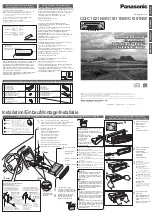
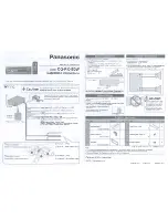
Summary of Contents for SLSW850 - PORT. CD PLAYER
Page 7: ......
Page 8: ......
Page 9: ......
Page 41: ...voltage input ...
Page 51: ...17 Packaging ...