5
2.2.
Service caution based on legal restrictions
2.2.1.
General description about Lead Free Solder (PbF)
The lead free solder has been used in the mounting process of all electrical components on the printed circuit boards used for this
equipment in considering the globally environmental conservation.
The normal solder is the alloy of tin (Sn) and lead (Pb). On the other hand, the lead free solder is the alloy mainly consists of tin
(Sn), silver (Ag) and Copper (Cu), and the melting point of the lead free solder is higher approx.30 degrees C (86
°
F) more than that
of the normal solder.
Definition of PCB Lead Free Solder being used
Service caution for repair work using Lead Free Solder (PbF)
• The lead free solder has to be used when repairing the equipment for which the lead free solder is used.
(Definition: The letter of “PbF” is printed on the PCB using the lead free solder.)
• To put lead free solder, it should be well molten and mixed with the original lead free solder.
• Remove the remaining lead free solder on the PCB cleanly for soldering of the new IC.
• Since the melting point of the lead free solder is higher than that of the normal lead solder, it takes the longer time to melt the
lead free solder.
• Use the soldering iron (more than 70W) equipped with the temperature control after setting the temperature at 350±30 degrees
C (662±86
°
F).
Recommended Lead Free Solder (Service Parts Route.)
• The following 3 types of lead free solder are available through the service parts route.
RFKZ03D01KS-----------(0.3mm 100g Reel)
RFKZ06D01KS-----------(0.6mm 100g Reel)
RFKZ10D01KS-----------(1.0mm 100g Reel)
Note
* Ingredient: tin (Sn), 96.5%, silver (Ag) 3.0%, Copper (Cu) 0.5%, Cobalt (Co) / Germanium (Ge) 0.1 to 0.3%
The letter of “PbF” is printed either foil side or components side on the PCB using the lead free solder.
(See right figure)
Summary of Contents for SDR-S50EB
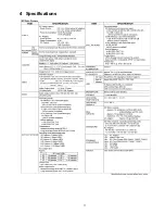
Page 11: ...11 4 Specifications ...
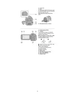
Page 13: ...13 ...
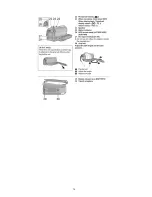
Page 14: ...14 ...
Page 18: ...18 7 Service Fixture Tools 7 1 Service Tools and Equipment ...
Page 21: ...21 Fig D3 Fig D4 ...
Page 24: ...24 Fig D13 Fig D14 Fig D15 Fig D16 ...
Page 25: ...25 Fig D17 Fig D18 Fig D19 Fig D20 ...
Page 26: ...26 Fig D21 Fig D22 ...
Page 28: ...28 8 4 1 How to use of CCD positioning pin RFKZ0476 ...
Page 30: ...30 9 2 2 Checking and repairing individual circuit boards How to use extension cables ...
Page 31: ...31 9 3 Location for Connectors of the Main P C B 9 3 1 Main P C B ...
Page 48: ...S 13 ...
Page 50: ...S 15 2 4 SDR T55 T56 T51 T50 S50 MONI FPC P C B ...
Page 52: ...S 17 4 4 21 20 19 18 17 16 15 14 13 12 11 SDR T55 T56 T51 T50 S50 MONI FPC P C B ...
Page 55: ...S 20 ...
Page 63: ...S7 2 LCD Section S 28 15 17 16 18 34 19 20 21 33 B17 B26 B27 ...


