background image

52

Summary of Contents for SA-PMX100

Page 1: ...nd Adjustment 4 1 3 Protection Circuitry 4 1 4 Caution For Fuse Replacement 4 1 5 Safety Part Information 4 2 Warning 5 2 1 Prevention of Electrostatic Discharge ESD to Electrostatically Sensitive ES Devices 5 2 2 Precaution of Laser Diode 5 2 3 Service caution based on Legal restrictions 6 2 4 Handling Precaution for Traverse Unit 6 Notes Please refer to the Original Service Manual for O CD Mecha...

Page 2: ... P C B 32 8 14 Disassembly of CD Mechanism Unit 32 8 15 Replacement of Traverse Unit 33 8 16 Disassembly of Bluetooth P C B 39 8 17 Disassembly of Rear Cabinet 39 9 Service Position 40 9 1 Checking of Panel Block Relay Antenna P C B and ALLPLAY Module 40 9 2 Checking of SMPS P C B 41 9 3 Checking of Main P C B 42 10 Block Diagram 45 10 1 SERVO SYSTEM CONTROL BLOCK DIAGRAM 45 10 2 AUDIO BLOCK DIAGR...

Page 3: ...ock hazards 1 1 1 Leakage Current Cold Check 1 Unplug the AC cord and connect a jumper between the two prongs on the plug 2 measure the resistance value with an ohmmeter between the jumpered AC plug and each exposed metallic cabinet part on the equipment such as screwheads connectors control shafts etc When the exposed metallic part has a return path to the chassis the reading should be between 1M...

Page 4: ...not operate unless the power is first turned off and then on again 1 4 Caution For Fuse Replacement 1 5 Safety Part Information Safety Parts List There are special components used in this equipment which are important for safety These parts are marked by in the Schematic Diagrams Exploded View Replacement Parts List It is essential that these critical parts should be replaced with manufacturer s s...

Page 5: ...vices are packaged with leads electrically shorted together by conductive foam aluminum foil or compara ble conductive material 7 Immediately before removing the protective material from the leads of a replacement ES device touch the protective material to the chassis or circuit assembly into which the device will be installed CAUTION Be sure no power is applied to the chassis or circuit and obser...

Page 6: ... be well molten and mixed with the original lead free solder Remove the remaining lead free solder on the PCB cleanly for soldering of the new IC Since the melting point of the lead free solder is higher than that of the normal lead solder it takes the longer time to melt the lead free solder Use the soldering iron more than 70W equipped with the temperature control after setting the temperature a...

Page 7: ...flexi ble cable cut off the antistatic FFC Figure 2 2 2 4 2 Grounding for electrostatic breakdown prevention Some devices such as the CD player use the optical pickup laser diode and the optical pickup will be damaged by static electricity in the working environment Proceed servicing works under the working environment where grounding works is completed 2 4 2 1 Worktable grounding 1 Put a conducti...

Page 8: ...ll allow service personnel s to understand and service this model Please place orders using the parts list and not the drawing reference numbers If the circuit is changed or modified this information will be followed by supplement service manual to be filed with original service manual 3 1 1 Firmware update ...

Page 9: ...192 kHz Audio word size 16 bits 24 bits Channel count 2 ch Ethernet interface LAN 10BASE T 100BASE TX Headphones Stereo 3 5 mm jack AUX IN EXT IN Pin jack Q Speaker Section Speaker unit s Woofer 14 cm cone type x 1 Tweeter 1 9 cm dome type x 1 Super tweeter 1 2 cm piezoelectric type x 1 Impedance 3 Ω Dimensions W x H x D 161 mm x 238 mm x 264 mm Mass Approx 3 kg Q Bluetooth Section Version Bluetoo...

Page 10: ...10 5 Location of Controls and Components 5 1 Main Unit Remote Control Key Button Operations ...

Page 11: ... inserted Step 2 Press and hold follow by on main unit for 2 second To exit press the TA on the main unit or using the remote control Unplug the AC cord Step 1 Press STOP on main unit To exit press the TA on the main unit or using the remote control Unplug the AC cord Step 1 Press and hold OK on remote control for more than 5 second To exit press the TA on the main unit or using the remote control...

Page 12: ...lay Remarks Error Code Diagnostic Contents Description of error D AMP IC output abnormal PDET2 DC_DET_AMP L NG PDET2 DC_DET_AMP is checked by reading the input 2x20ms F61 error code shall be memorized F76 Power supply abnormal PDET1 DC_DET_PWR L NG PDET1 DC_DET_PWR is checked by reading the input 2x1ms F76 error code shall be memorized Automatic FL Display Remarks Error Code Diagnostic Contents De...

Page 13: ...ersion will be display for 2 sec To enter into Doctor Mode for checking of various items and displaying EEPROM check sum and Opecon firmware version Note The Opecon firmware version as shown is an example It will be revised when there is updates Displaying of 1 Year of sales 2 Model type 3 ROM type 4 Opecon version number 5 SDK version 6 AllPlay version FL Display sequence Display 1 2 3 4 FL Displ...

Page 14: ...5 button on the remote control To exit Doctor Mode press DEL button on the remote control without power off Unplug the AC cord To cancel press 0 button on remote control CANCEL will be display and returns to Doctor Mode Press follow by 2 then 5 button on the remote control The NO DISC display will appear after 2s To activate cold start upon next power up Backup data are initialized Cold Start In D...

Page 15: ...ead back data NG will display Press follow by 1 then 6 button on the remote control AD value of region pin is check and display will show REG ON_YY based on region table YY 1 10 based on region table as below Checking for model no and Region Region Check NFC Data Writing NFC Data Test In Doctor Mode To exit Doctor Mode press DEL button on the remote control without power off Unplug the AC cord To ...

Page 16: ...Demo Step 1 Turn on the unit Step 2 Press and hold OPEN CLOSE and SELECTOR keys for 5 secs Step 3 The display will show entering into the mode Item FL Display Key Operation Mode Name Description Front Key To cancel Step 1 Select CD Mode and adjust volume level to 19 Step 2 Press and hold OPEN CLOSE and SELECTOR keys for 5 secs Step 3 The display will show after exit from the mode ...

Page 17: ...ire Switch between L and R speaker If no sound continues speakers are faulty Check value of resistance for speakers if it is пǡ speakers are faulty Table2 Yes Yes No Yes Yes Yes Yes No No No No Pin No 㩷 Waveform Output 㩷 㩷 4 㩷 㩷 4 㪄㪀㩷 㪊 㩷 㪋 㪣㩷㩿 㪀㩷 㩷 0 㩷 Table 2 PWM singnal output Pin28 31 36 39 from D AMP IC4200 is OK PWM singnal input Pin6 8 16 18 to D AMP IC4200 is OK PWM singnal output Pin27 28...

Page 18: ...y and J23 AllPlay OK Is 24P wire between CN8022 CN8021 Relay and J22 J23 AllPlay OK Is 24P wire between CN8020 Relay and CN8010 Main OK Check network connection and connection setting on smart phone or tablet refer to user s manual Replace Main P C B Replace Relay P C B Replace AllPlay Module Replace 24P wire Replace 20P and 30P wire 㩷 Item No Function P C B Module Bluetooth P C B NFC P C B Main P...

Page 19: ...s high temperature after prolong use Be sure to use proper service tools equipments or jigs during repair Select items from the following indexes when disassembly or replacement are required Disassembly of Top Cabinet Disassembly of Relay Block Disassembly of Dipole Antenna Disassembly of ALLPLAY Module Disassembly of Relay P C B Disassembly of Front Panel Unit Disassembly of Panel Block Disassemb...

Page 20: ...hart The following chart is the procedure for disassembling the casing and inside parts for internal inspection when carrying out the ser vicing To assemble the unit reverse the steps shown in the chart below 8 2 Type of screws ...

Page 21: ...21 8 3 Main Parts Location Diagram ...

Page 22: ...22 8 4 Disassembly of Top Cabinet Step 1 Remove 2 screws Step 2 Remove 3 screws Step 3 Adjust Dipole Antenna Step 4 Lift up to remove Top Cabinet ...

Page 23: ...y Block Refer to Disassembly of Top Cabinet Step 1 Remove 5 screws Step 2 Push inwards Dipole Antenna Step 3 Remove 2 screws and detach ground wire Step 4 Remove screw Step 5 Detach antenna wire at connector J2 on ALLPLAY Module ...

Page 24: ...h 7P wire at connector CN8254 on Relay P C B Step 7 Release 7P wire through groove at Support P C B Step 8 Detach 24P FFC at connector CN8020 on Relay P C B Step 9 Release guide Step 10 Lift up and remove Relay Block ...

Page 25: ...ve Step 2 Detach antenna wire at connector Ant1 on ALLPLAY Module Step 3 Lift up himelon Step 4 Remove Dipole Antenna 8 5 2 Disassembly of ALLPLAY Module Refer to Disassembly of Top Cabinet Refer to Disassembly of Relay Block Refer to Disassembly of Dipole Antenna Step 1 Detach 20P FFC at connector J22 on ALLPLAY Mod ule Step 2 Detach 30P FFC at connector J23 on ALLPLAY Mod ule Step 3 Remove 3 scr...

Page 26: ... Relay P C B Step 4 Remove 2 screws Step 4 Lift up Support P C B Relay P C B together and remove Relay P C B 8 6 Disassembly of Front Panel Unit Refer to Disassembly of Top Cabinet Step 1 Remove 2 screws and detach ground wire Step 2 Detach 7P wire at connector CN6000 on Main P C B Step 3 Detach 21P FFC at connector CN8001 on Main P C B Step 4 Detach 5P wire at connector CN4300 on Main P C B Step ...

Page 27: ...rt flathead screwdriver into both gaps Step 10 Apply light force at both gaps to lift up Front Panel Unit Step 11 Slightly lift forward and remove Front Panel Unit 8 7 Disassembly of Panel Block Refer to Disassembly of Top Cabinet Refer to Disassembly of Front Panel Unit Step 1 Remove Volume Knob Step 2 Remove Treble Knob Step 3 Remove Bass Knob ...

Page 28: ...mbly of NFC P C B Step 1 Remove NFC P C B from Panel P C B 8 7 2 Disassembly of Headphone P C B Step 1 Release ground wire from slot Step 2 Remove Headphone P C B 8 7 3 Disassembly of IR Sensor P C B Step 1 Remove Headphone P C B Step 2 Detach IR Sensor P C B at connector ZJ9200 from Panel Block Step 3 Remove IR Sensor P C B ...

Page 29: ...el Unit Step 1 Remove screw Step 2 Release wires from the guide Step 3 Release catch Step 4 Remove USB P C B 8 9 Disassembly of Antenna P C B Refer to Disassembly of Top Cabinet Refer to Disassembly of Front Panel Unit Refer to Disassembly of Panel Block Step 1 Release catch Step 2 Remove Antenna P C B ...

Page 30: ...Main P C B Refer to Disassembly of Top Cabinet Refer to Disassembly of Relay Block Refer to Disassembly of Front Panel Unit Step 1 Remove 2 screws Step 2 Remove PC Sheet Step 3 Detach 12P FFC at connector CN8008 on Main P C B Step 4 Detach 24P FFC at connector CN5002 on Main P C B Step 5 Detach 10P FFC at connector CN5001 on Main P C B Step 6 Detach 9P wire at connector CN8003 on Main P C B Step 7...

Page 31: ...efer to Disassembly of Front Panel Unit Refer to Disassembly of SMPS P C B Refer to Disassembly of Main P C B Step 1 Remove screw Step 2 Remove 2 screws Step 3 Lift up to release Inner Chassis from Rear Cabinet Caution During assembling ensure the Inner Chassis is fully inserted properly seated onto the catches ...

Page 32: ...o Disassembly of Inner Chassis Step 1 Remove screw Step 2 Remove Tuner P C B 8 14 Disassembly of CD Mecha nism Unit Refer to Disassembly of Top Cabinet Refer to Disassembly of Relay Block Refer to Disassembly of Front Panel Unit Refer to Disassembly of SMPS P C B Refer to Disassembly of Main P C B Refer to Disassembly of Inner Chassis Refer to Disassembly of Tuner P C B Step 1 Remove 2 screws Step...

Page 33: ...se Unit to prevent static damage to the Optical Pickup Unit Note 1 When the optical pickup unit is defective the overall traverse unit needs replacement 2 Please note that appropriate actions need to be taken to prevent static damage Step 1 Use a pin to slide Traverse Slide Plate until it come to a stop Step 2 Slide tray out fully Step 3 Release catches remove tray ...

Page 34: ...e the guide as shown slide Traverse Slide Plate to the end Step 5 Detach 5P FFC at the connector CN7001 on CD Interface P C B Step 6 Lift up Traverse Unit by approximately 45 Step 7 Remove traverse unit as arrow shown ...

Page 35: ...ace of the Optical Pickup Unit on the traverse unit 8 15 2 Assembly of Traverse Unit Step 1 Release the guide as shown slide Traverse Slide Plate to the end Step 2 Insert Traverse Unit at approximately 45 into mecha unit as arrow shown ...

Page 36: ... Unit properly into the grooves Step 4 Slide Traverse Slide Plate to lock the Traverse Unit as shown Step 5 Connect 5P FFC at connector CN7001 on CD Inter face P C B Step 6 Slide Traverse Slide Plate until it stop at the guide ...

Page 37: ...37 Step 7 Align and insert the tray into the mecha unit Step 8 Align the guides of the Traverse Slide Plate with the grooves when sliding the tray in Step 9 Slide the tray in fully ...

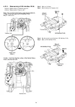
Page 38: ...o be short to prevent electrostatic dis charge during replacement of CD Interface P C B Step 1 Solder point Caution Avoid touching the surface of the Optical Pickup Unit on the Traverse Unit Step 2 Remove 2 screws Step 3 Attach short pin to Traverse Unit Step 4 Desolder points on solder side of CD Interface P C B Step 5 Remove CD Interface P C B ...

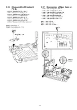
Page 39: ...ssembly of Tuner P C B Refer to Disassembly of CD Mechanism Unit Step 1 Remove screw Step 2 Remove Bluetooth P C B 8 17 Disassembly of Rear Cabinet Refer to Disassembly of Top Cabinet Refer to Disassembly of Relay Block Refer to Disassembly of Front Panel Unit Refer to Disassembly of SMPS P C B Refer to Disassembly of Main P C B Refer to Disassembly of Inner Chassis Refer to Disassembly of Tuner P...

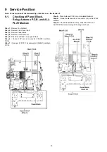
Page 40: ...ep 3 Remove Panel Block Step 4 Remove Antenna P C B Step 5 Place Panel Block on a support block Step 6 Connect 5P wire at connector CN4300 on Main P C B Step 7 Connect 21P FFC at connector CN8001 on Main P C B Step 8 Place Antenna P C B on an Insulated Material Step 9 Connect antenna wire at connector J2 on ALLPLAY Module Step 10 Check Panel Block Relay Antenna P C B and ALLPLAY Module according t...

Page 41: ...4 Remove Antenna P C B Step 5 Remove SMPS P C B Step 6 Place Panel Block on a support block Step 7 Connect 5P wire at connector CN4300 on Main P C B Step 8 Connect 21P FFC at connector CN8001 on Main P C B Step 9 Place Antenna P C B on an Insulated Material Step 10 Connect antenna wire at connector J2 on ALLPLAY Module ...

Page 42: ...tep 3 Remove Relay Block Step 4 Remove Panel Block Step 5 Remove Antenna P C B Step 6 Remove SMPS P C B Step 7 Remove Main P C B Step 8 Remove Inner Chassis Step 9 Remove Tuner P C B Step 10 Remove CD Mechanism Unit Step 11 Place Panel Block Main P C B SMPS P C B on an insulated material Step 12 Connect 15P wire at connector CN1100 on Main P C B Step 13 Connect 21P FFC at connector CN8001 on Main ...

Page 43: ...lace CD Mechanism Unit on an insulated material Step 16 Connect 10P FFC at connector CN5001 on Main P C B Step 17 Connect 24P FFC at connector CN5002 on Main P C B Step 18 Check Main according to the diagram shown ...

Page 44: ...44 ...

Page 45: ...P_OTW CD MECHANISM UNIT VOTR 10 VOTR CD LOADING P C B 6 CN5001 OPEN_SW 3 CN5001 CLOSE_SW 8 CN5001 LDM 7 CN5001 5 CN7002 8 CN7002 RESET_SW 4 CN5001 RESET_SW 7 CN7002 3 CN7002 4 CN7002 3 CN7001 1 CN7001 5 CN7001 4 CN7001 LDM SPM SPM 1 CN5001 SPM 2 CN5001 10 CN7002 9 CN7002 SPM TRV TRV 10 CN5001 TRV 9 CN5001 1 CN7002 2 CN7002 TRV OPEN_SW CLOSE_SW LDM LDM 9 RESET S7201 D D 5 CN6000 3 CN6100 D 6 CN6000...

Page 46: ...ONE P C B ALLPLAY MODULE RELAY P C B PANEL P C B IC4200 DIGITAL AUDIO PWM PROCESSOR IC4100 JK2000 A D CONVERTER IC2004 1Y 4 2 1A 2Y 7 5 2A 6 2B 3Y 9 11 3A 10 3B 1 SELECT 3 1B I2S_SEL_3 I2S_SEL_2 I2S_SEL_1 SEL_4 ASYNC_UNLOCK ADC_PON MD1 TU_RST TU_ SCL 1Y 4 2 1A 2Y 7 5 2A 6 2B 3Y 9 11 3A 10 3B 1 SELECT 3 1B 1Y 4 2 1A 2Y 7 5 2A 6 2B 3Y 9 11 3A 10 3B 1 SELECT 3 1B 1Y 4 2 1A 2Y 7 5 2A 6 2B 3Y 9 11 3A 1...

Page 47: ...DARY PRIMARY PW_VH PW_MOTOR5R6V PW_STBY3R3V PW_D3R3V IC2900 15V VOLTAGE REGULATOR MAIN P C B RESET IC8002 FROM TO SERVO SYSTEM CONTROL 5 6V SWITCHING VOLTAGE REGULATOR IC1102 D5812 D1105 D1104 D1113 D1100 D1103 D1101 D1110 D1102 L5713 2 3 1 4 1 VIN 2 ON OFF VOUT ADJ 5 4 5 CN1100 PCONT3 5 H2015 PCONT3 8 8 CN1100 H2015 15V 15V PW_MOTOR5R6V 5V A5V 5V PW_USB5R2V 5 2V PW_BT_5V 5V PW_STBY3R3V 3 3V DAMPV...

Page 48: ...V PW_D3R3V 16 6 CN9200 CN8001 PW_D3R3V PW_D3R3V PW_VH 5 17 CN9200 CN8001 PW_VH PW_VH 3 3V PW_STBY3R3V 3 3V PW_D3R3V VH PW_VH PW_MOTOR5R6V 3 19 CN9200 CN8001 FL FL FL FL 2 2 ZJ920 ZJ9200 PW_STBY3R3V PW_STBY3R3V 3 3V PW_STBY3R3V 1 1 CN4000 CN9201 PW_D3R3V PW_D3R3V 3 3V PW_D3R3V PW_D3R3V 9 CN8008 4 CN51 PW_D3R3V PW_3DR3V 3 3V PW_3 3V_MR 17 19 22 23 24 CN8010 1 2 3 6 8 CN8020 PW_3 3V_MR PW_3 3V_MR IR ...

Page 49: ...C B ALLPLAY MODULE MAIN P C B CN6100 7P CN51 12P CN7002 CN7001 10P 5P CN4000 5P CN7230 9P CN8001 CN6005 CN6000 P8001 CN8003 CN5001 CN5002 CN8008 21P 3P 2P 7P 9P 10P 24P CN8010 24P 12P CN4300 5P CN1100 15P ZJ9200 CN9202 4P 6P CN9201 P9200 CN9200 5P 5P 21P ZJ920 4P P8000 P8001 GND 6P 2P TO OPTICAL PICKUP UNIT CD MECHANISM UNIT CN8012 3P AC IN J2 2P F PANEL P C B D ANTENNA P C B J23 30P J22 20P Ant1 ...

Page 50: ...50 ...

Page 51: ...arts list In case of AC rated voltage Capacitors the part no and val ues will be indicated in the Schematic Diagram AC rated voltage capacitors C5700 C5701 C5702 C5705 C5706 Resistor Unit of resistance is OHM Ω K 1 000 M 1 000 000 Capacitor Unit of capacitance is μF unless otherwise noted F Farads pF pico Farad Coil Unit of inductance is H unless otherwise noted REF IS FOR INDICATION ONLY Voltage ...

Page 52: ...52 ...

Page 53: ...W SPM SPM LDM CLOSE_SW TRV LDM LDM OPEN_SW DGND REST_SW TRV LDM CLOSE_SW SPINDLE MOTOR M7301 TRAVERSE MOTOR R64 0 L54 0 R60 330 2 2K C69 10P C66 33P J0JHC0000118 LB52 R59 R67 0 R52 560 R51 2 2K 3P C67 IC52 LB51 J0JYC0000656 VA51 B0ZBZ0000156 L51 G1CR18JA0020 C51 1000P R56 220 R57 1K C62 0 1 C65 0 R55 220 7 9 10 8 4 5 1 3 2 6 12 11 CN51 10 C68 C61 0 1 G2 G3 G1 JK51 SDIO SCLK DGND RESET INT AUX_RCH ...

Page 54: ...XD MR_RXD PW_3R3V_MR PW_3R3V_MR PW_3R3V_MR FETX0_DPM FETX0_DPP JTAG_TCK JTAG_TDI FERX0_DPM FERX0_DPP PW_3R3V_MR PW_3R3V_MR V_ETH_CTAP MR_SCL I2C MR_SDA I2C PW_3R3V_MR HS_UART_TX PW_3R3V_MR GND GND GND GND GND SPI_CS GND SPI_CLK SPI_MOSI SPI_MISO MR_GPIO04 PW_3R3V_MR PW_3R3V_MR MR_LRCK I2S MR_BCK I2S MR_DATAIN I2S MR_MCLK I2S USBDATA_DPP USB_DATA_DPM MR_DATAOUT I2S MR_GPIO12 MR_GPIO11 I2C_SCL VCC R...

Page 55: ...OLLER IC8200 10P C8299 10P C8300 R6014 0 R6015 0 R6013 0 C6003 1000P 2 G2 1 4 G1 3 CN6004 0 1 C8304 10 R8298 2 2 C8277 22K R8340 5 6 1 3 4 2 8 7 CN8253 P7_6 WAKEUP0 P7_5 P7_4 VDDREG RESET RTC_ALARM RTCX2 VBAT P1_7 P1_9 P1_8 P1_4 P1_6 P1_5 P1_10 P5_3 P1_11 TDI DBGEN P0_1 P0_0 P4_9 TMS SWDIO TDO SWO TRST TCK SWDCLK TDI TMS TCK USB PORT PC IN FOR SOFTWARE DOWNLOAD TRST P4_1 P4_2 P4_7 P4_8 P4_4 P4_6 P...

Page 56: ... 18K R9215 R9272 39 R9271 47 R9270 47 10 R9254 33K R9273 C9253 0 1 C9251 0 1 1 C9252 10 R9253 B0ECKP000002 D9201 C9255 16V33 C9262 220P C9261 220P C9263 220P 38 5 1 6 7 2 8 9 27 28 29 30 31 32 33 34 35 11 12 13 14 15 16 17 10 18 19 21 22 23 24 25 26 20 39 R9252 30K C9259 50V10 C9254 0 1 HP_DET PLAY PAUSE DGND VH SDA SCL GND VDD KEY2 KEY1 DGND DGND BLUETOOTH PAIRING FWD REW F RCH HP_GND HP_GND OPEN...

Page 57: ...L LINE F TO PANEL CIRCUIT ZJ9200 IN SCHEMATIC DIAGRAM 4 F TO PANEL CIRCUIT CN9202 IN SCHEMATIC DIAGRAM 4 R920 47 R921 100 G2 2 1 3 G1 IR921 REMOTE CONTROL SENSOR 2 1 4 3 ZJ920 C920 1 DGND DGND REM_IN STBY_3 3V VCC VOUT GND 470 R8000 C8004 0 1 R8001 470 J0JGC0000070 LB8000 C8000 0 1 LB8001 J0JGC0000070 C8001 0 1 0 LB8002 7 6 3 4 2 1 5 JK8000 HEADPHONE 2 4 3 1 6 5 P8000 1 2 P8001 TO CHASSIS GND C800...

Page 58: ...0 4 2 1 3 5 C0DBAYH00005 12V VOLTAGE REGULATOR IC2900 1K R2909 C2906 16V820 C2907 35V56 8 9 13 11 10 12 2 3 1 5 7 6 4 15 14 H2015 47K R5868 0 1 C5870 R5728 22K 22K R5863 1 C5824 50V10 C5823 2 1 3 IC5823 C0DBGYY05244 5V VOLTAGE REGULATOR 1K R5867 R5818 10K 2 2K R5817 R5861 100K Q5863 B1ABGC000001 SWITCH R5801 100 DA2J10100L D5804 82K R5804 15K R5802 1 5K R5809 R5810 220 R5806 10K 10K R5805 C5828 6 ...

Page 59: ...2 R5704 1000P 1000P C5700 B0EAKT000063 D5702 R5703 100K C5713 1000P R5702 100K 3 1 2 D5802 B0HBSM000054 G2 G1 ZA2 0 R5866 C5805 35V470 R5701 470K R5700 470K R5710 470K C5712 400V82 B1ABCF000176 Q5761 27K R5768 D4CAA5R10001 TH5702 3 2 4 1 D5701 B0EDNR000001 DZ2J200M0L D5704 3 2 4 1 Q5720 B1BABG000007 VOLTAGE REGULATOR SWITCH 4 3 1 2 33K R5766 PC5721 FEEDBACK PC5761 FEEDBACK 4 3 1 2 DA2J10100L D5706...

Page 60: ...F PbF PbF PbF PbF CN6100 L6100 CN6101 3860AE 3860AE 3860AF 3860AF 3860AF 3860AF 3860AE 3860AE SPINDLE MOTOR M7302 CN7001 S7201 RESET TO LOADING P C B CD MECHANISM UNIT CN7002 M7301 TRAVERSE MOTOR 3556A 3556A USB PORT FM ANT 3860AC 3860AC 3860AC 3860AC TO MAIN P C B TO MAIN P C B TO ANTENNA R64 L54 L51 LB51 C68 C51 VA51 R67 R60 R59 R57 R56 R55 R52 R51 LB52 JK51 IC52 C69 C67 C66 C65 C62 C61 CN51 P80...

Page 61: ...200 IC8106 X8200 C8277 R8340 C8266 R8338 C7001 C7000 R8336 R8335 CN8254 R8334 CN8253 CN8022 CN8021 CN8020 CN7001 CN6004 R8327 R8324 R8323 R8322 R8321 R8316 R8313 R8312 R8311 R8310 R8309 R8308 R8307 R8306 R8305 R8304 R8302 R8301 R8300 R8298 R8294 R8287 R8286 R8285 C8329 R8284 R8279 C8325 C8323 R8274 C8322 R8273 C8321 R8272 C8320 R8271 C8319 R8270 C8318 R8269 C8317 R8231 C8316 R8230 C8315 R6015 C831...

Page 62: ...2 R9271 R9270 R9255 R9258 R9256 R9257 LB9201 R9203 R9205 R9204 R9206 R9201 R9211 LB9202 Q9201 Q9202 Q9203 R9267 R9268 R9269 R9266 R9265 R9264 C9215 C9211 C9214 C9210 R9216 R9220 R9217 R9215 R9221 R9218 R9253 C9253 R9254 R9273 C9254 C9251 C9252 R9252 C9261 C9262 C9263 R9261 R9262 R9263 R9202 C9200 C9202 LB9203 C9257 W124 W125 R9313 POWER STOP PLAY PAUSE REW FWD BT OPEN CLOSE SELECTOR LB8001 LB8002 ...

Page 63: ...906 W16 C5823 ZA2 HEATSINK R5808 R5801 C5818 R5768 C5817 C5800 W24 R5767 C5791 W23 R5882 R5766 C5761 W22 C5760 W21 R5868 R5764 D5710 W20 R5867 R5763 D5812 D5707 W26 R5866 R5762 D5807 D5706 R5864 D5804 D5705 C5730 R5863 Q5864 D5704 R5862 R5733 Q5863 R5861 R5732 Q5761 R5728 Q5760 R5819 R5818 QR5862 R5817 R5722 C5870 R5721 C5869 R5814 R5720 QR5762 R5710 R5810 R5704 R5809 R5703 R5702 D5760 C5724 R5701...

Page 64: ...64 ...

Page 65: ... reference information when probing defect point because it may differ from actual measuring value due to difference of Measuring instrument and its measuring condition and product itself 14 1 MAIN SUPPLY P C B REF NO MODE 1 2 4 6 8 8 POWER ON 5 0 0 98 3 3 0 26 REF NO MODE 1 2 4 6 8 8 POWER ON 5 0 0 96 3 3 0 26 REF NO MODE 2 3 4 5 6 POWER ON 2 0 8 3 3 5 6 3 3 REF NO MODE 1 2 3 4 5 6 7 8 POWER ON 5...

Page 66: ...0 0 REF NO MODE 1 2 3 POWER ON 26 5 0 0 REF NO MODE E C B E C B E C B E C B E C B POWER ON 3 3 1 2 3 3 5 0 3 3 1 2 0 0 5 0 0 4 2 0 3 3 3 3 5 0 STANDBY 3 3 1 2 3 3 5 0 3 3 1 2 0 0 5 0 0 4 2 0 3 3 3 3 5 0 REF NO MODE E C B E C B E C B E C B POWER ON 0 0 1 2 4 4 12 9 4 4 13 4 4 12 9 0 3 3 0 STANDBY 0 0 1 2 4 4 12 9 4 4 13 4 4 12 9 0 3 3 0 SA PMX100EG SMPS P C B Q5760 QR5822 Q5864 QR5862 QR5762 Q5720 ...

Page 67: ... CN8253 CN8022 CN8021 CN8020 CN8012 CN8010 CN8008 CN8003 CN8001 CN7230 CN7002 CN7001 CN7001 CN6101 CN6100 CN6005 CN6004 CN6000 CN5002 CN5001 CN4300 CN4201 CN4200 CN1100 CN51 MECHANISM UNIT 310 310 301 58 57 56 55 54 53 52 51 50 50 50 50 50 49 48 47 46 45 44 41 40 40 39 38 37 37 36 36 35 35 35 35 35 35 35 34 34 33 33 33 31 31 30 30 30 30 30 29 29 29 29 29 29 29 29 29 29 29 29 29 29 28 27 26 25 24 2...

Page 68: ... PMX100EG ACCESSORIES BAG P3 P2 P2 FRONT P1 A5 x 2 SPEAKER CABLE A4 FM INDOOR ANTENNA A3 O I BOOK AC CORD A2 A1 REMOTE CONTROL SC PMX100EG PACKAGING DRAWING 1 2 3 4 5 6 7 8 9 A B C D E F G H 10 11 12 13 P2 POLYFOAM LEFT POLYFOAM RIGHT ...

Page 69: ... RMB0993 CD LID SPRING 1 19 RMGX0033 CUSHION RUBBER 2 20 RMK0812 1 BOTTOM CHASSIS 1 21 RMK0898 INNER CHASSIS 1 22 RMQ2423 PC SHEET 1 23 RMQ2463 SMPS PC SHEET 1 24 RMQX0382 3 CD MECHA SUPPORT 2 25 RMX0539 SMPS SPACER 1 26 RSC1097 D AMP HEAT ABSORBER 1 27 RSC1305 THERMAL PAD 1 28 RMN1059 FL HOLDER 1 29 XTB3 8JFJ SCREW 14 30 RHD26046 L SCREW 5 31 RHD30007 1SJ SCREW 2 33 RHD30111 31 SCREW 3 34 RHDX031...

Page 70: ...RMF0797 HIMELON 1 TRAVERSE DECK 301 RAE1047Z V TRAVERSE ASS Y 1 E S D 310 XTN2 6GFJ SCREW 2 PACKING MATERI ALS P1 RPG0Q43 2 PACKING CASE 1 P2 RPN2733 POLYFOAM 1 P3 RPFX1012 1 BAG 1 ACCESSORIES A1 N2QAYB001018 REMOTE CONTROL 1 A2 K2CQ2YY00119 AC CORD 1 A3 RQT9992 1D O I BOOK Ge It Fr Du Da Sw Fi 1 A3 RQT9993 1E O I BOOK 1 A3 RQT9994 1R O I BOOK Po Cz Sp 1 A3 RQT9995 1B O I BOOK En 1 A4 RSAX0002 FM ...

Page 71: ...201 MFI337S3959 IC 1 E S D IC8202 C1CB00004388 IC 1 E S D TRANSISTORS Q5720 B1BABG000007 TRANSISTOR 1 E S D Q5760 B1ADCF000001 TRANSISTOR 1 E S D Q5761 B1ABCF000176 TRANSISTOR 1 E S D Q5863 B1ABGC000001 TRANSISTOR 1 E S D Q5864 B1ABGC000001 TRANSISTOR 1 E S D Q9201 B1ABCF000176 TRANSISTOR 1 E S D Q9202 B1ABCF000176 TRANSISTOR 1 E S D Q9203 B1ABCF000176 TRANSISTOR 1 E S D QR5762 B1GBCFJA0006 TRANSI...

Page 72: ...NDUCTOR 1 LB5830 J0JHC0000107 INDUCTOR 1 LB8000 J0JGC0000070 INDUCTOR 1 LB8001 J0JGC0000070 INDUCTOR 1 LB8163 J0JHC0000118 INDUCTOR 1 LB8164 J0JYC0000656 INDUCTOR 1 LB8165 J0JYC0000656 INDUCTOR 1 LB8166 J0JYC0000656 INDUCTOR 1 LB8167 J0JYC0000656 INDUCTOR 1 LB8268 J0JYC0000656 INDUCTOR 1 LB8269 J0JYC0000656 INDUCTOR 1 Safety Ref No Part No Part Name Description Qty Remarks TRANSFORMERS T5701 G4DYZ...

Page 73: ...290 D0GA103JA023 10K 1 16W 1 R8291 D0GA103JA023 10K 1 16W 1 Safety Ref No Part No Part Name Description Qty Remarks R8292 D0GAR00J0005 0 1 16W 1 R8293 D0GDR00J0004 0 1 8W 1 R8294 D0GA101JA023 100 1 16W 1 R8295 D0GA101JA023 100 1 16W 1 R8298 D1BB1002A074 10K 1 10W 1 R8299 D0GAR00J0005 0 1 16W 1 R8300 D0GAR00J0005 0 1 16W 1 R8301 D0GA222JA023 2 2K 1 16W 1 R8302 D0GA222JA023 2 2K 1 16W 1 R8304 D0GA10...

Page 74: ...8 F1G1C104A146 0 1uF 16V 1 C8289 F1G1C104A146 0 1uF 16V 1 C8290 F1G1C104A146 0 1uF 16V 1 C8291 F1G1C104A146 0 1uF 16V 1 C8292 F1G1C104A146 0 1uF 16V 1 C8293 F1G1C104A146 0 1uF 16V 1 C8294 F1G1C104A146 0 1uF 16V 1 C8295 F1G1C104A146 0 1uF 16V 1 C8296 F1G1C104A146 0 1uF 16V 1 C8297 F1G1C104A146 0 1uF 16V 1 C8298 F1G1C104A146 0 1uF 16V 1 C8299 F1G1H100A834 10pF 50V 1 C8300 F1G1H100A834 10pF 50V 1 C83...

Reviews: