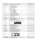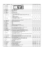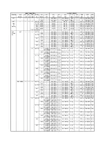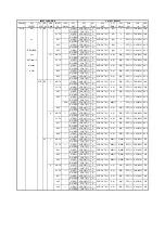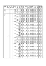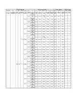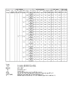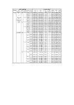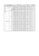
Pin No.
Signal Name
I/O
Describe
P-OFF P-SAVE P-FAIL
Reset
31
POS.SW3
I
In
In
In
In
32
POS.SW2
I
In
In
In
In
33
POS.SW1
I
In
In
In
In
34
RESET(L)
I
MICOM reset input terminal.
In
In
In
In
35
32KHz IN
I
Sub oscillator input.
---
---
---
---
36
32KHz OUT
O Sub oscillator output.
---
---
---
---
37
+5V(D)
-
Power.
---
---
---
---
38
12MHz.IN
I
Main oscillator input.
---
---
---
---
39
12MHz.OUT
O Main oscillator output.
---
---
---
---
40
GND(D)
-
---
---
---
---
41
POWER OFF(L)
O
Control signal for power circuit.
*Low is existed when turning off the power supply for concerned circuit.
*High is existed while power is supplied to mechanism and/or concerned circuit,
although it
seems to be power off.
Low
Low
Low
Low
42
FIP ON(L)
O
Control signal for FIP on/off.
P-OFF in power save mode: "H" is output.
Other than above: "L" is output.
(Output switching timing of FIP"L" is same with the switching timing of POWER OFF
"L".)
Low
High
Low
Low
43
12M.START(H)
I
Starting clock select terminal at releasing RESET.
---
---
---
---
44
LC.OSC IN
I
OSC terminal for OSD dot clock.
---
---
---
---
45
LC.OSC OUT
O OSC terminal for OSD dot clock.
---
---
---
---
46
GND
I
GND
---
---
---
---
47
4FC.LPF
I
NC
---
---
---
---
48
OSD.FSC IN
I
NC
---
---
---
---
49
GND(OSD)
-
GND
---
---
---
---
50
CVIN
I
Composite video signal input terminal.
---
---
---
---
51
LECHA
I
Composite video signal white level input terminal.
---
---
---
---
52
CVOUT
O CG video output teminal.
---
---
---
---
53
5V(OSD)
-
---
---
---
---
54
HLF
I
LPF connection terminal for SLICER (Used for OSD dot clock.)
---
---
---
---
55
AMUTE(H)
O Audio mute signal only for RF convertor.
High
High
Low
High
56
CVIN(EDS)
I
Composite video signal input terminal for SLICER.
In
In
In
In
57
GND
I
---
---
---
---
58
SECAM/PAL(SYS2)
O Output terminal for the unit recognition result of broad cast system.
Low
Low
Low
Low
59
SECAM.V.IN
I
Chroma input terminal for SECAM SUPERIMPOSE.
---
---
---
---
60
OSD PULSE
O Abstraction signal for BOX from the video signal at SUPERIMPOSE.
Low
Low
Low
Low
61
SLEEP(L)
O
Power circuit control signal for super power save mode.
*P-OFF in power save mode: "L" is output.
Other than above: "H" is output.
*Output switching timing of FIP "L" is same with the switching timing of POWER OFF
"L".)
High
Low
Low
High
62
UNLOADING(H)
O
Control signal for Loading motor forward.
*High is existed when the loading motor rotates reverse direction and/or breaking.
Low
Low
Low
Low
63
LOADING(H)
O
Control signal for Loading motor reverse.
*High is existed when the loading motor rotates forward direction and/or breaking.
Low
Low
Low
Low
64
FLD CS
O FLD chip select terminal.
Not fix
Not fix
Low
Low
65
MESECAM DET(H)
I
Detection between MESECAM and NORMAL in playback mode.
In
In
In
In
66
LP(H)
O
Output signal depens on tape speed in both EE and VV modes.
* During N4H,N6H,P6H or P9H: High.
* Other than above speed: Low.
Low
Low
Low
Low
67
NC
O
Non connect.
* Low fixed.
Low
Low
Low
Low
68
FLD DATA OUT
O Serial data output signal for FIP driver.
Not fix
Not fix
Low
Low
69
FLD DATA IN
I
Serial data input signal for FIP driver.
Not fix
Not fix
In
In
70
FLD CLK
O Serial clock signal for FIP driver.
Not fix
Not fix
Low
Low
71
IIC CLK
O IIC clock for all IIC devices
Not fix
Not fix
Low
Low
72
IIC DATA
O IIC data for all IIC devices
Not fix
Not fix
Low
Low
73
125Hz
O
125Hz output for adjustment of clock accuracy .
(Output in only TEST MODE 2.)
Low
Low
Low
Low
74
CAP.R/F
O Control signal for capstan motor diriction.
Low
Low
Low
Low
Input terminal for mechanism position.
D.A.REC(H)
BIAS(L)
140mS
140mS

