background image

 1. Turn on the PC and install the TATSUJIN Adjustment

Program into the PC.

 2. TATSUJIN PC-Adjustment Program start in the following

procedure.
PC Menu : [Start]

[Program]

[win Tatsujin]

[DV

Movie]

[NV-GS230 Series]

Fig. E5-1

The main menu display will be displayed.

 3. Select the desired model.
 4. Turn on the camcorder. Then, click “Start.”

Fig. E5-2

 5. The communication is complete, and the dialog will appear.

Then, click “VCR (V) or Cam (C)” to save the EEPROM
data,

Fig. E5-3

 6. Saving for EEPROM data is complete, menu will appear.

To perform each adjustment, display the adjustment menu
by selecting the desired menu from “Camera Adjust,”
“Video Adjust,” “LCD Adjust” or “EVF Adjust” and select
each adjustment item.

Fig. E5-4

Note:

The adjustment data is stored to the EEPROM IC after
each adjustment.

 7. After adjustment, to end the software, select “Exit” in File

menu or close the window.

Fig. E5-5

6.3. SET-UP PC-EVR ADJUSTMENT PROGRAM

28

NV-GS230EG

Summary of Contents for NV-GS230E

Page 1: ...reserved Unauthorized copying and distribution is a violation of law NV GS230EG NV GS230E NV GS230EB NV GS230EP NV GS230EF NV GS230EK NV GS230GC NV GS230GN NV GS238GK VOL 1 A MECHANISM Colour S Silver Type Digital Video Camera Recorder ORDER NO VM0701012CE ...

Page 2: ...2 NV GS230EG ...

Page 3: ...ERALL SCHEMATIC DIAGRAM 35 10 2 INTERCONNECTION SCHEMATIC DIAGRAM 36 10 3 SIDE L FLEX CARD CASSETTE COVER SCHEMATIC DIAGRAM 38 10 4 LCD HINGE MONITOR FLEX SCHEMATIC DIAGRAM 38 10 5 REAR OPERATION UNIT SCHEMATIC DIAGRAM 38 10 6 EVF SCHEMATIC DIAGRAM 38 10 7 CCD FLEX CARD SCHEMATIC DIAGRAM 39 10 8 FRONT SCHEMATIC DIAGRAM 40 10 9 JACK SCHEMATIC DIAGRAM 41 10 10 SIDE R LCD DET SCHEMATIC DIAGRAM 42 10 ...

Page 4: ...ram and P C B layout of Main P C B Sub P C B 2 Parts List for individual parts of Main P C B Sub P C B 2 The following category is are recycle module part Please send it them to Central Repair Center Main P C B VEP03G73AA NV GS230EG E EB EP EF VEP03G73AB NV GS230EK VEP03G73AC NV GS230GC GN VEP03G73AD NV GS238GK Sub P C B VEP23670A NV GS230EG E EB EP EF EK GC GN GS238GK When a part replacement is r...

Page 5: ...er has to be used when repairing the equipment for which the lead free solder is used Definition The letter of PbF is printed on the PCB using the lead free solder To put lead free solder it should be well molten and mixed with the original lead free solder Remove the remaining lead free solder on the PCB cleanly for soldering of the new IC Since the melting point of the lead free solder is higher...

Page 6: ...not be used until a replacement cover is obtained A replacement fuse cover can be purchased from your local Panasonic Dealer If the fitted moulded plug is unsuitable for the socket outlet in your home then the fuse should be removed and the plug cut off and disposed of safety There is a danger of severe electrical shock if the cut off plug is inserted into any 13 ampere socket If a new plug is to ...

Page 7: ...ent Type No ML 621S F9D Manufactured by Panasonic It must never be subjected to excessive heat or discharge It must therefore only be fitted in equipment designed specifically for its use Replacement batteries must be of the same type and manufacture They must be fitted in the same manner and location as the original battery with the correct polarity contacts observed Do not attempt to re charge t...

Page 8: ... 4 1 DISASSEMBLE FLOW CHART This flow chart indicates the disassembly steps the cabinet parts P C B and Mecha Unit in order to access to be serviced When reinstalling perform the steps in the reverse order Fig F1 8 NV GS230EG ...

Page 9: ...201 FP2202 FP2203 FP2204 FP5001 FP6501 FP6504 FP6505 1 Screw K 4 Tabs Main P C B 6 Mecha Unit Fig D11 Open the Cassette Cover 3 Screws L Mecha Unit 7 Jack P C B Fig D12 1 Screw M 1 Screw N 1 Screw O Jack P C B 8 Front P C B Fig D13 5 Screws P 3 Tabs Front P C B 9 Monitor P C B Fig D14 1 Screw Q 3 Screws R Rear Cover Fig D15 Turning the LCD Unit 2 Screws S LCD Unit Fig D16 2 Screws T 6 Tabs LCD Cas...

Page 10: ...Fig D3 Fig D4 Fig D5 Fig D6 10 NV GS230EG ...

Page 11: ...Fig D7 Fig D8 Fig D9 11 NV GS230EG ...

Page 12: ...Fig D10 Fig D11 Fig D12 Fig D13 12 NV GS230EG ...

Page 13: ...Fig D14 Fig D15 Fig D16 Fig D17 13 NV GS230EG ...

Page 14: ...Fig D18 Fig D19 Fig D20 Fig D21 14 NV GS230EG ...

Page 15: ...Fig D22 Fig D23 15 NV GS230EG ...

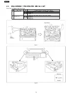
Page 16: ...al Screw Connector Flex Other 1 Cassette Up Unit Fig M1 It makes the mechanism position in Eject condition For Battery Fig M2 3 Screws A Fig M3 3 Tabs I remove the piece arrangement unit from rail department 2 Cylinder Unit Fig M4 1 Screw B Fig M5 3 Screw C Cylinder Unit Fig M1 Fig M2 16 NV GS230EG ...

Page 17: ...Fig M3 17 NV GS230EG ...

Page 18: ...Fig M4 Fig M5 18 NV GS230EG ...

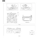
Page 19: ...Fig M6 19 NV GS230EG ...

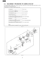
Page 20: ... following flowchart describes order or steps for removing the Camera lens unit and certain printed circuit boards in order to make access to the item needing service To reassemble the unit follow the steps in reverse order Fig L1 Fig L2 20 NV GS230EG ...

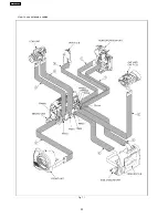
Page 21: ...according to the Movie Camera s suffix Then confirm and or adjust the VTR and Camera section one by one 5 2 SERVICE EXTENSION CABLES This models is required the following extension cables for all connections Note 1 Use the following extension cables when checking or adjusting individual circuit boards except module Parts Main P C B and Sub P C B 21 NV GS230EG ...

Page 22: ...How to use extension cables Fig T1 22 NV GS230EG ...

Page 23: ...E FP2203 K1MN18BA0060 FP6502 K1MN14BA0061 FP6504 K1MN27BA0058 FP5001 K1MN08BA0107 IC2006 EEPROM 1 4 8 5 FP6505 K1MN21BA0058 FP6501 K1MN12BA0059 FP2202 K1MN10BA0067 FP2204 K1MN08BA0060 FP1001 K1MN14BA0062 PP3001 K1KA20BA0052 FP2201 K1MN18BA0067 PS3001 K1KBC0A00037 FP6503 K1MN26A00068 23 NV GS230EG ...

Page 24: ...5 3 2 SUB P C B FOIL SIDE COMPONENT SIDE FP602 K1MN27BA0058 FP201 K1MN39BA0058 FP701 K1MN21BA0058 FP601 K1MN22A00065 PP301 K1KAC0A00014 IC307 EEPROM 1 4 8 5 24 NV GS230EG ...

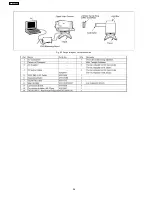
Page 25: ...e effective model s TATSUJIN Software to PC Personal Computer 2 SET UP CONNECTION a Remove the EVR cover of the DV Camcorder Unlock the locking tab and remove the EVR cover as shown in Fig E1 b Make a connection Connect the PC the PC IF Unit and the DV Camcorder as shown in Fig E2 and E3 c Check the SW position on Measuning Board The position of SW on Measuning Board checks as shown in Fig E4 Fig ...

Page 26: ...Fig E3 Rough image of set up connection 26 NV GS230EG ...

Page 27: ...Fig E4 Extension cables VFK1317 2pcs Measuring Board VFK1308E 232C I F Cable VFK1395 27 NV GS230EG ...

Page 28: ...complete and the dialog will appear Then click VCR V or Cam C to save the EEPROM data Fig E5 3 6 Saving for EEPROM data is complete menu will appear To perform each adjustment display the adjustment menu by selecting the desired menu from Camera Adjust Video Adjust LCD Adjust or EVF Adjust and select each adjustment item Fig E5 4 Note The adjustment data is stored to the EEPROM IC after each adjus...

Page 29: ...IAL GUIDELINE The table below shows which adjustments are necessary according to the unit parts and individual parts to be replaced Make sure to perform these adjustments shown below as necessary 29 NV GS230EG ...

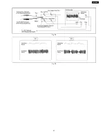
Page 30: ...1 is connected to EVR adjustment board as shown in Fig D2 4 The enbelope detection spcial tool board is connected to oscilloscope as shown in Fig D2 5 The post is adjusted with the post driver VFK1899 so that recycles the normal tape which recorded NTSC signal and the detection wave link become a flat as shown in Fig D3 At the time of the clyinder unit exchange unnecessary 6 The post is adjusted w...

Page 31: ...Fig D2 Fig D3 31 NV GS230EG ...

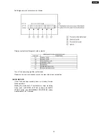
Page 32: ...n and PHOTO SHOT button simmultaneously for 3 seconds 3 Operating automatic diagnosis cord is displayed Item 3 is selected with the JOYSTICK UP or DOWN button NO is selected with the JOYSTICK RIGHT button YES is selected with the JOYSTICK UP or DOWN button Press the CURSOR CENTER button Fig S1 NOTE Do not operate items Except for 3 in the Service Menu 8 SERVICE MODE PUSH THE RESET SWITCH is displa...

Page 33: ...g mode push JOYSTICK LEFT button and QUICK START button and RECORDING START STOP button simultaneously for 3 seconds Self diagnosis cord contents are as follows Display contents self diagnosis cord contents Turn off the power supply after confirmation Please do the error cord backup record the clear after repair completion 33 NV GS230EG ...

Page 34: ...9 WAVEFORM TABLE R908 REC PLAY 3 0Vp p 20usec div R909 REC PLAY 3 0Vp p 20usec div R907 REC PLAY 3 0Vp p 20usec div 34 NV GS230EG ...

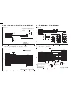
Page 35: ...IDEO OUTPUT NV GS230 GS238 OVERALL SCHEMATIC DIAGRAM FOCUS CCD IC601 CONTROLLER SIGNAL PROCESSOR LCD IC107 110 INVERTER IC108 V DRIVER IC102 REG IC103 REG 2FCK X101 IC104 105 106 CDS AGC AD IC303 DIGTAL SIGNAL PROCESSOR IC305 CAMERA MICROCOMPUTER IC701 IRIS DRIVE AF ZOOM DRIVE IC307 EEPROM SUB POWER LENS DRIVE MONITOR P C B EVF P C B 0 33 LCD IC3201 RIP MODULATION VITERBI EQ MOTOR DRIVE CONTROL IC...

Page 36: ...GND GUI LED VTR KEY 2 VTR KEY 1 GND SS SW DEW 1 2 3 4 5 6 7 8 9 10 11 12 13 14 CARD PRO CARD DET SD DATA1 SD DATA0 CMD O 26 25 22 23 24 POWER LCD RESET P LCD LED REG D3V LCD DET VTR KEY 4 CARD LED GND GND TPB TPB TPA TPA DSC GND DSC GND DSC GND SD CLK O SD D33V 1 2 3 4 5 6 7 8 9 10 11 12 13 14 15 16 17 18 SD D33V SD DATA2 SD DATA3 19 20 21 FP6503 20 19 18 17 16 15 14 13 12 11 10 9 CAM VD SYSTEM RS...

Page 37: ... D GND 10 M OEVE M FR D GND D GND D GND M PWM M LED 5V M LED 5V D GND 27 E CKV1 3 22 26 E DSG 19 8 D GND 20 E XSTV 10 E DSD EVF 8 5V 21 E CKH1 9 6 4 7 11 1 E XSTH 16 E STH 12 E CKH2 E G OUT 5 E R OUT 13 E B OUT E STV E CKV2 14 E COM EVF BL 5V 15 22 17 18 21 25 23 24 E XENB E XDSG E ENB 2 FP601 M CKH2 M H L M CKH1 M OEV M PCG M OEVE M FR M VCSH M CKV M STV M CSV M B M R M G M CSH M STH M 8 5V M COM...

Page 38: ...P QUICK START 5 7K 2 84K REV FF SET PLAY 17 36K 5 7K 2 84K FP6502 TO 10K 10K 10K 10K TAPE REC TAPE PLAY CARD REC PICTURE PLAY PC POWER DEW DEW SS SW GND VTR KEY 1 VTR KEY 2 GUI LED GND REG D3V VTR KEY 3 STANDBY LED POWER LED POWER SW MAIN CONNECTION TO 14 13 12 11 10 9 8 7 6 5 4 3 2 1 5 REAR OPERATION UNIT 2 C A B 4 1 3 NV GS230 GS238 REAR OPERATION UNIT SCHEMATIC DIAGRAM 10 6 EVF SCHEMATIC DIAGRA...

Page 39: ... 6 7 8 9 10 11 12 5V 18 17 16 15 14 13 V3 V2 V4 H1 H2 SUB R PT PT 15V 15V A GND V1 A GND SIG A GND A GND SIG B A GND A GND SUB B H2 B H1 B V4 B V3 B V2 B V1 B 5V B 5V B PT PT SIG G 15V 15V R SUB G H2 G H1 G V4 G V3 G V2 G V1 G A GND A GND A GND A GND SUB R H2 R H1 R V4 R V3 R 39 38 37 36 35 34 33 32 31 30 29 28 27 26 25 24 23 22 21 20 19 18 17 16 15 14 13 12 11 10 9 8 7 6 3 2 1 4 5 SIG R V1 R 5V R...

Page 40: ...R6401 OUT GND VCC 1 2 3 330K R492 AMP B1ABCF000100 Q491 0 22 C492 0 22 C493 10M R495 MA3S132D0L D491 3 2 1 2 2M R491 B3GA00000039 D6802 0 1 C491 R FILTER B1ABBE000002 Q4803 4700 R4815 6V22 C4808 33K R4814 4 7 C4807 22K R4813 MIC AMP NJM2115V IC4801 0 047 C4802 680P C4804 56K R4806 0 R4804 680P C4803 56K R4805 0 R4803 0 047 C4801 3900 R4802 3900 R4801 D4ED1270A003 VZ4801 D4ED1270A003 VZ4802 VCC GND...

Page 41: ...0 R4918 AMP 6V22 C4910 470 R4912 1 C4908 10K R4913 150K R4914 1K R4916 AMP AMP 2SB1462JHL Q4902 2SD2216J0L Q4901 5600 R4910 150 R4911 6V22 C4905 1K R4909 150K R4907 10K R4906 470 R4905 1 C4903 56K R4908 4700P C4003 4700P C4004 C4001 1 LB4003 J0JAC0000014 LB4005 J0JAC0000014 LB4001 J0JBC0000054 LB4006 J0JAC0000014 LB4921 J0JAC0000015 LB4926 J0JAC0000015 LB4924 J0JAC0000015 LB4923 J0JAC0000015 2 3 S...

Page 42: ...C DET GND 13 14 9 1 2 3 4 5 6 7 8 12 11 10 J0MAB0000116 FL3953 4 3 1 2 J0MAB0000116 FL3952 4 3 2 1 CARD PRO CARD DET SD DATA1 SD DATA0 CMD O SD DATA3 SD DATA2 SD D33V SD D33V SD CLK O DSC GND DSC GND DSC GND TPA TPA TPB TPB GND GND CARD LED VTR KEY 4 LCD DET REG D3V P LCD LED RESET POWER LCD FP6503 25 FP6503 24 FP6503 23 FP6503 22 FP6503 21 FP6503 20 FP6503 19 FP6503 18 FP6503 17 FP6503 16 FP6503 ...

Page 43: ...M VSS G V COM V COM CKD2 CKD1 VVSS VREF OEV PCG OEVE FR VCSH CKV STV CSV B R D GND D GND D GND D GND M LED 5V M LED 5V M PWM M CKH2 M CKH1 M OEV M PCG M OEVE M FR M VCSH M CKV M STV M CSV M B M R M G M CSH M STH M 8 5V M COM 1 2 3 4 5 6 7 8 9 10 11 12 13 14 15 16 17 18 19 20 21 22 23 24 25 FP902 MONITOR FLEX TO VIDEO MAIN SIGNAL PATH MONITOR P C B 9 8 7 6 5 4 3 2 1 F E D C B A NV GS230 GS238 MONIT...

Page 44: ...NV GS230EG 44 ...

Page 45: ... NV GS230 GS238 EVF P C B 11 2 LCD DET P C B VEP001H9A COMPONENT SIDE FOIL SIDE 1 A B 2 3 4 5 NV GS230 GS238 LCD DET P C B 11 3 SIDE R P C B COMPONENT SIDE FOIL SIDE 1 A B C D E F 2 3 4 VEP001S4A NV GS230 GS238 SIDE R P C B 11 CIRCUIT BOARD ASSEMBLIES NV GS230EG 45 ...

Page 46: ...0GC NV GS230 GS238 CCD FLEX CARD P C B COMPONENT SIDE FOIL SIDE NOTE MULTILAYER P C B THIS P C B IS Multi Layer P C B THIS CIRCUIT BOARD SHOWS COMPONENT LAYOUT PATTERN FOR COMPONENT SIDE AND FOIL SIDE LAYOUT PATTERNS ARE SINGLE PATTERN FOR EACH SIDE THAT MAKE EASY TO SIGHT THE COMPONENT LAYOUT NV GS230EG 46 ...

Page 47: ...IS Multi Layer P C B THIS CIRCUIT BOARD SHOWS COMPONENT LAYOUT PATTERN FOR COMPONENT SIDE AND FOIL SIDE LAYOUT PATTERNS ARE SINGLE PATTERN FOR EACH SIDE THAT MAKE EASY TO SIGHT THE COMPONENT LAYOUT VEP04881C 1 A B C D E 2 3 4 5 6 7 8 9 NV GS230 GS238 FRONT P C B NV GS230EG 47 ...

Page 48: ...E 6 C3908 C 2 CL4002 D 5 C4001 C 2 CL4003 C 6 C4003 F 5 CL4004 D 6 C4004 F 5 CL4901 C 5 C4901 D 5 CL4902 D 5 C4902 E 5 RL2501 F 1 C4903 E 5 RL2502 E 6 C4904 E 5 RL2503 A 5 C4905 E 1 RL2504 A 2 C4906 D 1 RL4801 E 1 C4908 D 5 Connector C4909 D 5 FP6201 C 5 C4910 E 2 Jack C4913 E 5 JK3001 B 2 Resistor JK3901 C 3 R4001 D 5 JK4001 F 2 R4901 D 5 JK4901 D 2 R4902 D 1 Diode R4904 D 5 D4901 D 1 R4905 E 5 A...

Page 49: ...11 7 MONITOR P C B VEP08335A 1 A B C D E F 2 3 4 5 6 7 8 COMPONENT SIDE FOIL SIDE NV GS230 GS238 MONITOR P C B NV GS230EG 49 ...

Page 50: ...NV GS230EG 50 ...

Page 51: ...12 EXPLODED VIEWS 12 1 FRAME CASING SECTION 1 51 NV GS230EG ...

Page 52: ...12 2 FRAME CASING SECTION 2 52 NV GS230EG ...

Page 53: ...12 3 LCD SECTION 53 NV GS230EG ...

Page 54: ...12 4 CAMERA LENS SECTION 54 NV GS230EG ...

Page 55: ...12 5 VCR MECHANISM SECTION 55 NV GS230EG ...

Page 56: ...12 6 PACKING PARTS ACCESSORIES SECTION 56 NV GS230EG ...

Page 57: ...6 VHD1775 SCREW 1 B7 VHD1642 SCREW 1 B8 VHD1642 SCREW 1 B9 XQN16 BJ4FN SCREW 1 B10 VHD1393 SCREW 1 Ref No Part No Part Name Description Pcs Remarks B11 VHD1393 SCREW 1 B12 XQN16 B5FN SCREW 1 B13 XQN16 BJ6FN SCREW 1 B14 XQN16 BJ6FN SCREW 1 B15 XQN16 BJ6FN SCREW 1 B16 XQN14 BJ5FJK SCREW 1 B18 XQN16 BJ35FN SCREW 1 B19 XQN16 BJ35FN SCREW 1 B20 XQN16 BJ35FN SCREW 1 B21 XQN16 B3FN SCREW 1 B22 XQN16 B3FN...

Page 58: ...REW 1 B303 XQN16 CJ7FJ SCREW 1 B304 XQN16 CJ7FJ SCREW 1 B305 XQN16 CJ7FJ SCREW 1 B306 XQN16 CJ5FJ SCREW 1 B307 XQN16 CJ5FJ SCREW 1 B308 XQN16 CJ5FJ SCREW 1 Ref No Part No Part Name Description Pcs Remarks B309 XQN16 CJ5FJ SCREW 1 B310 XQN16 CJ5FJ SCREW 1 B311 XQN16 CJ5FJ SCREW 1 B312 XQN16 CJ5FJ SCREW 1 13 5 VCR MECHANISM SECTION PARTS LIST Ref No Part No Part Name Description Pcs Remarks 501 VXK1...

Page 59: ...Ref No Part No Part Name Description Pcs Remarks R4801 ERJ6GEYG392 M RESISTOR CH 1 10W 3 9K 1 R4802 ERJ6GEYG392 M RESISTOR CH 1 10W 3 9K 1 R4803 D0YAR0000007 M RESISTOR CH 1 16W 0 1 R4804 D0YAR0000007 M RESISTOR CH 1 16W 0 1 R4805 ERJ2GED563X M RESISTOR CH 1 16W 56K 1 ERJ2RHD563X R4806 ERJ2GED563X M RESISTOR CH 1 16W 56K 1 ERJ2RHD563X R4807 ERJ2GEJ103 M RESISTOR CH 1 16W 10K 1 R4808 ERJ2GEJ103 M R...

Page 60: ... 1 VZ4003 D4ED1270A008 SURGE ABSORBER 1 VZ4004 D4ED1270A006 SURGE ABSORBER 1 VZ4902 D4ED1120A002 SURGE ABSORBER 1 VZ4903 D4ED1120A002 SURGE ABSORBER 1 n VEP001S4A SIDE R P C B RTL C6301 F1H0J475A010 C CAPACITOR CH 6 3V 4 7U 1 C6302 F1G1H470A566 C CAPACITOR CH 50V 47P 1 Ref No Part No Part Name Description Pcs Remarks C6303 F1G1H470A566 C CAPACITOR CH 50V 47P 1 C6304 F1G1H470A566 C CAPACITOR CH 50V...

Page 61: ... ERJ3GEYJ331 M RESISTOR CH 1 10W 330 1 R908 ERJ3GEYJ331 M RESISTOR CH 1 10W 330 1 R909 ERJ3GEYJ331 M RESISTOR CH 1 10W 330 1 R910 ERJ3RBD822 M RESISTOR CH 1 16W 8 2K 1 R912 ERJ3RBD102 M RESISTOR CH 1 16W 1K 1 R913 ERJ3RBD472 M RESISTOR CH 1 16W 4 7K 1 R915 D0GB102JA057 M RESISTOR CH 1 10W 1K 1 R918 ERJ3RED270 M RESISTOR CH 1 16W 27 1 R924 ERJ3RED270 M RESISTOR CH 1 16W 27 1 R925 ERJ3RED270 M RESIS...

Reviews: