background image

105

KX-TG6421HGT/KX-TGA641FXT

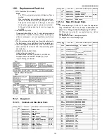
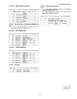
15.5.3.2. Main P.C.Board Parts

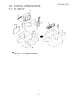
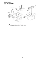
15.5.4. Accessories and Packing Materials

Note:

(*1) You can download and refer to the Operating  Instruc-
tions (Instruction book) on TSN Server.

15.5.4.1. KX-TG6421HGT

15.5.4.2. KX-TGA641FXT

15.5.5. Screws

15.5.6. Fixtures and Tools

Note:

(*1) See 

Equipment Required

 (P.60), and 

The Setting

Method of JIG (Handset)

 (P.64).

(*2) When replacing the Handset LCD, See 

How to

Replace the Handset LCD

 (P.59).

T.I

KXTG6421HGT

KXTGA641FXT

Safety

Ref. 

No.

Part No.

Part Name & Description Remarks


PCB200 PQWPTGA721CH 

MAIN P.C.BOARD ASS'Y
(RTL)


(DIODE)

D1     B0JAME000095 DIODE(SI)

(JACK)

J1     K2ECYB000001 JACK   

S

(RESISTOR)

R1     ERG2SJ100E    10


(FUSE)

F1     K5H302Y00003 FUSE

Safety Ref. 

No.

Part No.

Part Name & Description Remarks

A1     PQLV219CEX        AC ADAPTOR


A2     PQJA10075Z        CORD, TELEPHONE 


A3

PNQX1676Z         INSTRUCTION BOOK (*1) 


A4

PNQW1524Z          LEAFLET, QUICK GUIDE        

P1     PQPP10152Z        

PROTECTION COVER (for
Base Unit)    


P2     XZB08X25B02       

PROTECTION COVER (for
Handset)    


P3     PNPK2266Z         GIFT BOX  


Safety Ref. 

No.

Part No.

Part Name & Description Remarks

A101   PQLV219CEX        AC ADAPTOR


A102   PNQX1700Z         

INSTRUCTION BOOK (for
English) (*1) 


A103   PNQX1851Z         

INSTRUCTION BOOK (for
Arabic) (*1)   

P101   XZB08X25B02       

PROTECTION COVER (for
Handset)    


P102   XZB13X19C03       

PROTECTION COVER (for
Charger Unit)    


P103   PNPK1892Z         GIFT BOX  


Safety

Ref. 

No.

Part No.

Part Name & Description Remarks

 A

XTB26+8GFJ

TAPPING 

SCREW

B

XTB2+8GFJ

TAPPING SCREW

Safety

Ref. 

No.

Part No.

Part Name & Description Remarks

PQZZ1CD300E JIG CABLE (*1)


PNZZTG6421HG BATCH FILE CD-ROM (*1)


PQZZ430PIR

TIP OF SOLDERING IRON
(*2)


PQZZ430PRB

RUBBER OF SOLDERING
IRON (*2)  


Summary of Contents for KX-TGA641FXT

Page 1: ...ons Co Ltd 2009 Unauthorized copying and distribution is a viola tion of law ORDER NO KM40904889CE Telephone Equipment Model No KX TG6421HGT KX TGA641FXT Digital Cordless Answering System T Titanium Black Version for Hungary ...

Page 2: ...2 KX TG6421HGT KX TGA641FXT ...

Page 3: ...0 2 How to Replace the Handset LCD 59 11 Measurements and Adjustments 60 11 1 Equipment Required 60 11 2 The Setting Method of JIG Base Unit 60 11 3 Adjustment Standard Base Unit 62 11 4 Adjustment Standard Charger Unit 63 11 5 The Setting Method of JIG Handset 64 11 6 Adjustment Standard Handset 66 11 7 Things to Do after Replacing IC or X tal 67 11 8 RF Specification 69 11 9 How to Check the Han...

Page 4: ...d by the manufacturer 3 Dispose of used batteries according to the manufacture s Instructions 2 2 About Lead Free Solder Pbf Pb free Note In the information below Pb the symbol for lead in the periodic table of elements will refer to standard solder or solder that con tains lead We will use PbF solder when discussing the lead free solder used in our manufacturing process which is made from Tin Sn ...

Page 5: ...d Bismuth Sn Zn Bi Please check the manufacturer s specific instructions for the melting points of their products and any precautions for using their product with other materials The following lead free PbF solder wire sizes are recommended for service of this product 0 3 mm 0 6 mm and 1 0 mm 2 3 Discarding of P C Board When discarding P C Board delete all personal information such as telephone di...

Page 6: ... 3 Specifications Note Design and specifications are subject to change without notice Note for Service Operation range Up to 300 m outdoors Up to 50 m indoors depending on the condition Analog telephone connection Telephone Line ...

Page 7: ... Encoding Burst Decoding RF PLL 5 3 77 75 9 10 EEPROM SCL SDA 57 58 44 To AC Adaptor Limit Resistor Charge Detector CHARGE CONTACT Optional VUNREG 3 0V Reg IC1 2 4V Reg Q9 1 8V Reg Q8 3 0 V 2 4 V 1 8 V BBIC IC401 IC7 KX TG6421 BLOCK DIAGRAM BASE UNIT MOD DEMOD Charge Pump 43 2 5V XTAL X1 10 368 MHz IC801 RX n RX p TX p TX n P on PSEL V DD PADRV 4 3 6 7 TX on RX on D801 6 72 ANT1 ANT2 9 8 ANT1 ANT2...

Page 8: ...lation and Echo suppression DSP section Any tones tone sidetone ringing tone etc generation DSP section DTMF receiver DSP section Clock Generation for RF Module ADC DAC timer and power control circuitry PLL Oscillator Detector Compress Expander First Mixer All interfaces ex RF Power Amp EEPROM LED Analog Front End etc RF Power Amp IC801 Amplifier for transmission and reception EEPROM IC401 Tempora...

Page 9: ... shown in Fig 101 The power supply is as follows DECT BBIC IC7 DC Jack 6 5 V D1 IC1 IC7 DC Jack 6 5 V D1 IC1 Q9 IC7 DC Jack 6 5 V D1 IC1 Q8 IC7 RF Power Amp IC801 DC Jack 6 5 V D1 IC1 IC801 Power AMP EEPROM IC401 DC Jack 6 5 V D1 IC1 IC7 IC401 FLASH MEMORY IC421 DC Jack 6 5 V D1 IC1 IC7 IC421 Charge Contact TP16 DC Jack 6 5 V D1 R56 R55 D22 TP16 Fig 101 ...

Page 10: ... IC7 as shown in Block Diagram Base Unit P 7 The voice signal passes through the analog part of IC7 where it is amplified and converted to a digital audio stream signal The burst switch controller processes this stream performing encryption and scrambling adding the various other fields to produce the GAP Generic Access Profile standard DECT frame assigning to a time slot and channel etc In IC7 th...

Page 11: ...5 15 16 19 20 32 31 57 58 36 13 43 42 63 54 55 66 ADPCM Codec Filter DSP Speech Decoding Speech Encoding BMC Burst Decoding RF PA ANT1 IC801 Burst Encoding RF PLL MOD DEMOD 5 3 4 3 6 7 8 9 2 77 78 75 RXn RXon ANT1 DA801 RXp TXp TXn Pon PSEL TXon VDD PADRY 9 10 XTAL X1 10 368 MHz BATTERY 44 ON SWITCH KEYPAD Charge Pump ROWS COLUMNS CP3 0 V CP4 0 V 48 49 50 51 22 23 24 25 26 BBIC IC1 IC3 56 LCD BACK...

Page 12: ... 4 3 Charge Circuit Circuit Operation When charging the handset on the Base Unit the charge current is as follows DC 6 5 V D1 R56 R55 D22 CHARGE Base CHARGE Handset Q4 D7 F1 BATTERY Bat tery BATTERY R45 GND CHARGE Handset CHARGE Base GND DC GND In this way the BBIC on Handset detects the fact that the battery is charged The charge current is controlled by switching Q9 of Handset Refer to Fig 101 i...

Page 13: ...13 KX TG6421HGT KX TGA641FXT 4 5 Circuit Operation Charger Unit 4 5 1 Power Supply Circuit The power supply is as shown ...

Page 14: ...14 KX TG6421HGT KX TGA641FXT 4 6 Signal Route ...

Page 15: ...15 KX TG6421HGT KX TGA641FXT ...

Page 16: ...16 KX TG6421HGT KX TGA641FXT 5 Location of Controls and Components 5 1 Controls 5 1 1 Base Unit 5 1 2 Handset ...

Page 17: ...17 KX TG6421HGT KX TGA641FXT 6 Installation Instructions 6 1 Connections 6 2 Battery 6 2 1 Battery Installation See For Service Hint P 27 6 2 2 Battery Charge ...

Page 18: ... correctly if the battery is disconnected and connected again even after it is fully charged In that case by recharging the battery as mentioned above you will get a correct indication of the battery strength 6 2 3 Battery Level 6 2 4 Panasonic Ni MH Battery Performance supplied batteries ...

Page 19: ...421HGT KX TGA641FXT 7 Operating Instructions 7 1 Programmable Settings You can customise the unit by programming the following features using the handset 7 1 1 Programming by scrolling through the display menus ...

Page 20: ...hen pressing and keys Refer to How to Clear User Setting P 34 2 The item will not be reset when pressing and keys Refer to How to Clear User Setting P 34 Cross Reference Registering a Handset to a Base Unit P 21 7 1 2 Answering System Setting 7 1 3 SMS Setting ...

Page 21: ...e When you purchase an additional handset refer to the additional handset s installation manual for registration Cross Reference For Service Hint P 27 7 2 1 Deregistering a Handset 7 3 Copying Phonebook Entries You can copy phonebook entries to the phonebook of another compatible Panasonic handset 7 3 1 Copying all entries ...

Page 22: ...22 KX TG6421HGT KX TGA641FXT 7 4 Dialling mode 7 5 Error Messages ...

Page 23: ...23 KX TG6421HGT KX TGA641FXT 7 6 Troubleshooting ...

Page 24: ...24 KX TG6421HGT KX TGA641FXT ...

Page 25: ...25 KX TG6421HGT KX TGA641FXT ...

Page 26: ...26 KX TG6421HGT KX TGA641FXT ...

Page 27: ...27 KX TG6421HGT KX TGA641FXT 7 7 For Service Hint Cross Reference Battery Charge P 17 ...

Page 28: ...28 KX TG6421HGT KX TGA641FXT 8 Service Mode 8 1 Engineering Mode 8 1 1 Base Unit ...

Page 29: ... dB up When hex changes from 00 0B to 00 16 or 00 2C gain increases by 6 dB or 12 dB Frequency 00 02 00 01 02 70 Use these items in a READ ONLY mode to confirm the contents Careless rewriting may cause serious damage to the computer system ID 00 10 00 14 Given value Bell length 01 F7 32 5sec 3 1E 3 sec 14 2 sec This is time until bell stops ringing Unit 100 ms PULSE Dial speed 10PPS 20PPS 03 9F 21...

Page 30: ...30 KX TG6421HGT KX TGA641FXT 8 1 2 Handset ...

Page 31: ... cause serious damage to the handset Items Address Default Data New Data Possible Adjusted Value MAX hex Possible Adjusted Value MIN hex Remarks Sending level 00 06 Adjusted value Given value 6F 00 2 Receiving level 00 07 Adjusted value Given value 00 3F 3 Battery Low 00 04 70 4 Frequency 00 02 00 01 02 70 ID 00 10 00 14 Given value Desired Number hex Input Keys Desired Number hex Input Keys 0 0 A...

Page 32: ...r has registered Available models KX TG6421 Refer to the following procedures Note BS Base Unit HS Handset If the max number of handsets are already registered to the base unit a new handset cannot be registered To register the handset refer to Registering a Handset to a Base Unit P 21 To cancel the handset refer to Deregistering a Handset P 21 To copy the handset phonebook refer to Copying Phoneb...

Page 33: ...sets are already registered to the base unit a new handset cannot be registered To register the handset refer to Registering a Handset to a Base Unit P 21 To cancel the handset refer to Deregistering a Handset P 21 To copy the handset phonebook refer to Copying Phonebook Entries P 23 ...

Page 34: ... Resetting both base unit and handset Both the base unit and the registered handset which you did the following steps to are reset Other registered handsets will not be reset Note 1 Refer to Registering a Handset to a Base Unit P 21 8 3 2 Resetting only handset The only handset is reset by doing the following steps to Note 2 The handset registration to the base unit is cancelled If the handset nee...

Page 35: ...oting Flowchart Flow Chart Cross Reference Check Power P 36 Bell Reception P 46 Check Battery Charge P 37 Check Link P 38 Check the RF part P 42 Check Handset Transmission P 45 Check Handset Reception P 45 Signal Route P 14 Check Caller ID P 45 Check TAM Operation P 46 ...

Page 36: ... 1 Base Unit Is the AC Adaptor inserted into AC outlet 1 Cross Reference Power Supply Circuit P 9 Note 1 Refer to Specifications P 6 for part number and supply voltage of AC Adaptor 9 1 1 2 Handset Cross Reference Power Supply Circuit Reset Circuit P 12 ...

Page 37: ...X TGA641FXT 9 1 2 Check Battery Charge 9 1 2 1 Base Unit Cross Reference Charge Circuit P 12 9 1 2 2 Handset Cross Reference Check Power P 36 Charge Circuit P 12 9 1 2 3 Charger Unit Cross Reference Charge Circuit P 12 ...

Page 38: ... KX TG6421HGT KX TGA641FXT 9 1 3 Check Link 9 1 3 1 Base Unit Note 1 Refer to Troubleshooting by Symptom Base Unit and Charger Unit P 47 Cross Reference Check Point Base Unit P 47 Power Supply Circuit P 9 ...

Page 39: ...39 KX TG6421HGT KX TGA641FXT Cross Reference Check Point Base Unit P 47 ...

Page 40: ...40 KX TG6421HGT KX TGA641FXT 9 1 3 2 Handset Note 1 Refer to Troubleshooting by Symptom Handset P 51 Cross Reference Check Point Handset P 51 Power Supply Circuit Reset Circuit P 12 ...

Page 41: ...41 KX TG6421HGT KX TGA641FXT Cross Reference Check Point Handset P 51 ...

Page 42: ... 9 1 4 1 Finding out the Defective part After All the Checkings or Repairing 1 Re register the checked Handset to the checked Base Unit and Regular HS to Regular BU Note If you need to register a handset refer to Registering a Handset to a Base Unit P 21 ...

Page 43: ... 2 RF Check Flowchart Each item 1 3 of RF Check Flowchart corresponds to Check Table for RF part P 44 Please refer to the each item Note 1 Base unit refer to G of Check Point Base Unit P 47 Handset refer to H of Check Point Handset P 51 ...

Page 44: ...be checked to Regular BU 2 Press Talk key of the HS to establish link 2 X tal Frequency confirmation 1 Check X tal Frequency 1 10 368 MHz 100 Hz 1 Check X tal Frequency 2 10 368 MHz 100Hz 3 Range Confirmation Normal HS BU Mode Normal mode 1 Register Regular HS to BU to be checked 2 Press Talk key of the Regular HS to establish link 3 Compare the range of the BU being checked with that of the Regul...

Page 45: ... 5 Check Handset Transmission Cross Reference Signal Route P 14 9 1 6 Check Handset Reception Cross Reference How to Check the Handset Speaker or Receiver P 70 Signal Route P 14 9 1 7 Check Caller ID Cross Reference Signal Route P 14 ...

Page 46: ...lephone Line Interface P 10 Check Link P 38 How to Check the Handset Speaker or Receiver P 70 9 1 9 Check TAM Operation Cross Reference Power Supply Circuit P 9 Note 1 When replacing FLASH MEMORY IC421 TAM data need to be written to it Refer to Base Unit of Things to Do after Replacing IC or X tal P 67 ...

Page 47: ...e current value 3 Adjust the 1 8V voltage of VDD1 executing command VDD XX XX is the value Q8 C75 C614 C61 IC7 C Charge Pump 2 5V Supply Confirma tion VDD5 1 Confirm that the voltage between test point VDD5 and GND is 2 5 V 0 1 0 3 V IC7 C625 C631 D Charge Pump 3 0V Supply Confirma tion VDD4 1 Confirm that the voltage between test point VDD4 and GND is 3 0 V 0 2 V IC7 C616 C630 E BBIC Confirmation...

Page 48: ... command sendchar TST 3 Execute the command sendchar dmv 2 2 4 Check that Signalling Status has been set to Locked then press ACCEPT RFPI 5 Initiate connection from Dect tester set up connect 6 Execute the command ANT1 7 Confirm that the NTP value at ANT is 19 0 dBm 25 0 dBm IC7 C802 C806 C808 C814 C820 C819 C822 C823 C825 C827 C826 C834 C851 C853 C859 C861 DA801 DA802 IC801 L801 L803 C855 C858 R8...

Page 49: ...861 DA801 DA802 IC801 L801 L803 C855 C858 R801 R807 R106 R109 Q9 C617 O Timing Confirmation ANTI_TP Follow steps 1 to 6 of J 7 Confirm that the Timing accuracy is 5 0 ppm When adjust the frequency of CLK in item G 15 ppm When do not adjust the frequency of CLK in item A IC7 C802 C806 C808 C814 C820 C819 C822 C823 C825 C827 C826 C834 C851 C853 C859 C861 DA801 DA802 IC801 L801 L803 C855 C858 R801 R8...

Page 50: ...s 5 at Receiver Volume Middle 150 Ω Load IC7 SA1 L1 L2 D3 Q3 Q4 R14 R15 R16 R17 D21 Q5 R19 R20 C14 C56 R117 R116 C141 R9 C22 C23 R Charging Check 1 Connect Charge Contact 12 Ω 2 W resistor between charge and charge 2 Measure and confirm voltage across the resistor is 3 10 V 0 3 V R55 R56 D22 D23 S TAM Operation Confir mation 1 TAM Confirmation Execute the command sendchar VPI 2 Confirm the returne...

Page 51: ...5 C40 C45 F1 B BBIC Confirmation 1 BBIC Confirmation Execute the command getchk 2 Confirm the returned checksum value Connection of checksum value and program number is shown below IC1 X1 RA61 R64 R66 C EEP ROM Confirmation 1 EEP ROM Confirmation Execute the command sendchar EPV 2 Confirm the returned Value Value for reference is written at EEPROM C SUM in Software_Version_Table xls IC1 IC3 R40 R4...

Page 52: ... 3 Check X tal Frequency 10 368 MHz 100 Hz 4 If the frequency is not 10 368 MHz 100 Hz adjust the frequency of CLK exe cuting the command sendchar sfr xx xx where xx is the value so that the reading of the frequency counter is 10 368000 MHz 5 Hz Note Clear the registered information for Base Unit before measurement because the Frequency will not possibly get stable due to the registered informatio...

Page 53: ... mA 3 Input 45 dBm 1KHz to MIC and measure Line output level 4 Confirm that the level is 8 5 dBm 2 dBm and that the distortion level is 5 at TEL Line 600 Ω Load 5 Input 20 dBm 1KHz to Line I F and measure Receiving level at REV and REV 6 Confirm that the level is 21 dBm 2 dBm and that the distortion level is 5 at Receiver vol 2 IC1 C12 D19 D20 C96 C97 R215 R27 RA4 C11 C13 R28 D3 D4 MIC L9 RA2 R73 ...

Page 54: ... customer s line has less line loss ex The customer is using optical fiber ISDN terminal adaptor or PBX In this case receiving signal is strong and it may affect transmission signal 2 When the other party is talking from noisy place ex The other party is using cellular phone The background noise is very loud In this case the noise from the other party i e surrounding noise may affect transmission ...

Page 55: ...55 KX TG6421HGT KX TGA641FXT 10 Disassembly and Assembly Instructions 10 1 Disassembly Instructions 10 1 1 Base Unit ...

Page 56: ...56 KX TG6421HGT KX TGA641FXT ...

Page 57: ...57 KX TG6421HGT KX TGA641FXT 10 1 2 Handset ...

Page 58: ...58 KX TG6421HGT KX TGA641FXT 10 1 3 Charger Unit ...

Page 59: ...59 KX TG6421HGT KX TGA641FXT 10 2 How to Replace the Handset LCD ...

Page 60: ...ass production 11 2 The Setting Method of JIG Base Unit This section explains the PC setting to use command required in Check Point Base Unit P 47 Preparation Serial JIG cable PQZZ1CD300E PC which runs in DOS mode Batch file CD ROM for setting PNZZTG6421HG Note If you have the JIG Cable for TCD500 series PQZZ1CD505E change the following values of resis tance Then you can use it as a JIG Cable for ...

Page 61: ...M Type rdeeprom 00 00 FF and the data from address 00 00 to FF is read out readid Read ID RFPI Type readid and the registered ID is read out writeid Write ID RFPI Type writeid 00 18 E0 0E 98 and the ID 0018 E0 0E 98 is written hookoff Off hook mode on Base Type hookoff hookon On hook mode on Base Type hookon getchk Read checksum Type getchk wreeprom Write the data of EEPROM Type wreeprom 01 23 45 ...

Page 62: ...855 C52 C169 C170 C136 C171 C168 C149 C74 C837 C75 C145 C146 C150 C858 R20 R23 R18 R24 R116 R12 R13 R35 R32 R87 R86 L2R L1R L2T L1T BLK YLW RED GRN TP10 D23 D26 D21 Q2 C622 C14 C57 R19 R117 R29 R2 TP9 D22 D16 D15 Q5 GND_C Q8 C615 C430 C60 C630 C616 R424 R425 R430 R426 R429 R428 R427 IC421 TP16 sub TP16 TP15 sub TP15 RA80 RA1 GND LINE_DC GND CHARGE CHARGE GND RX TX L1T Q Q I Q A B C D T R G DTMF Te...

Page 63: ...n connecting the simulator equipment for checking please refer to below 11 4 1 Bottom View Note A is referred to Check Point Charger Unit P 50 TP4 TP3 1 2 J1 D1 A F1 PbF PQLV30055 PQLV30056 PQUP11532Z Charge Charge 10 2 W Digital Volt Meter A DC POWER DC 6 5 V TP3 TP4 GND ...

Page 64: ...IG Cable for TCD500 series PQZZ1CD505E change the following values of resis tance Then you can use it as a JIG Cable for both TCD300 and TCD500 series It is an upper compatible JIG Cable 11 5 1 Connections Connect the DC Power or Battery to BATT and BATT Connect the JIG cable GND black to GND Connect the JIG cable UTX yellow to UTX and URX red to URX Note COM port names may vary depending on what ...

Page 65: ...on Example rdeeprom Read the data of EEPROM Type rdeeprom 00 00 FF and the data from address 00 00 to FF is read out readid Read ID RFPI Type readid and the registered ID is read out writeid Write ID RFPI Type writeid 00 18 E0 0E 98 and the ID 0018 E0 0E 98 is written getchk Read checksum Type getchk wreeprom Write the data of EEPROM Type wreeprom 01 23 45 01 23 is address and 45 is data to be wri...

Page 66: ...4 R31 R7 R6 R4 R45 L804 L4 L8 L5 RA2 RA4 RA61 D22 D21 D13 D14 D1 D7 D4 D3 Q11 Q12 Q9 C862 C105 C187 C186 C107 C106 C103 C104 C580 C175 C860 C182 C859 C36 C45 C820 C825 C861 C 8 0 8 C809 C810 C805 C806 C812 C827 L801 L803 C803 C819 C826 C822 TEST C46 C33 C109 C111 C16 C12 C14 C97 C96 C184 C18 C47 C17 Q2 R215 C41 C13 C11 C188 C50 C49 C108 C39 C110 C127 C128 C83 C185 C82 C15 C150 C3 F1 C121 C74 C75 C...

Page 67: ...loading has finished 6 Detach the JIG cable then disconnect the DC Power 7 Connect the DC Power 8 Connect the JIG cable again and execute the command getchk then confirm the checksum value is correct If the downloading fails start again from step 1 9 Default batch file Execute the command default bat 10 Country version batch file Execute the command TG6421XXrevYY bat 1 11 Clock adjustment Refer to...

Page 68: ... Detach the JIG cable then press the handset Power key to turn it on 8 Connect the JIG cable again and execute the command getchk then confirm the checksum value is correct If the downloading fails start again from step 1 10 Default batch file Execute the command default bat 11 Default batch file remaining Execute the command TGA641DEFrevYY bat 3 12 Country version batch file Execute the command T...

Page 69: ...Frequency Drift 35 kHz ms Check Point Base Unit M RX Sensitivity 1000 ppm Check Point Base Unit N Timing Accuracy 5 0 ppm 15 0ppm Check Point Base Unit O Power RAMP Power RAMP is matching Check Point Base Unit P Item Value Refer to TX Power 19 dBm 25 dBm Check Point Handset I Modulation 370 30 370 30 kHz div Modulated width 690 kHz Check Point Handset J Frequency Offset 50 kHz 50 kHz Check Point H...

Page 70: ...ndset BASE UNIT HANDSET Channel No Transmit Frequency Receive Frequency Transmit Frequency Receive Frequency 1 1897 344 1897 344 1897 344 1897 344 2 1895 616 1895 616 1895 616 1895 616 3 1893 888 1893 888 1893 888 1893 888 4 1892 160 1892 160 1892 160 1892 160 5 1890 432 1890 432 1890 432 1890 432 6 1888 704 1888 704 1888 704 1888 704 7 1886 976 1886 976 1886 976 1886 976 8 1885 248 1885 248 1885 ...

Page 71: ... A I A I 27 ADC1 INT0 P1_0 A I ADC1 A I A I 28 NTC ADC2 GND A I 29 SOCp GND A I 30 SOCn GND A I 31 CHARGE_CTRL A O N C A O O 0 32 P1_7 CHARGE A I CHARGE I I 33 PAOUTp P3_1 A O PAOUTp A O O 0 34 VDDPA VDDPA 35 PAOUTn P3_0 A O PAOUTn A O O 0 36 VBAT1 VBAT1 37 CP_C1x A I O N C A I O A I 38 CP_C2x A I O CP_C2x A I O A I 39 CP_C1y A I O N C A I O A I 40 VBAT2 VBAT2 41 CP_C2y A I O CP_C2y A I O A I 42 C...

Page 72: ... C O_0 O 0 67 P2_1 ECZ2 PWM1 LED4 D O LED2 A I A I 68 P2_0 ECZ1 PWM0 LED3 D O LED1 A I A I 69 VDD2 1 8V 70 LDORF_CTRL A I LDORF_CTRL A I A I 71 RF_SUPPLY2 RF_SUPPLY2 72 RF0n D O ANT2 O_0 1 Hi Z 73 RFP4 D O PON O_0 1 Hi Z 74 RFP3 D O PSEL O_0 1 Hi Z 75 VDD_PADR A O VDD_PADRV A O A O 76 VSS_PADR1 GND 77 RF_TXp A O TXp A O A O 78 RF_TXn A O TXn A O A O 79 VSS_PADR2 GND 80 RFP2 TXON Hi Z 81 GND GND Pi...

Page 73: ...28 NTC ADC2 A I ADC2 I_0 A I 29 SOCp A I SOCp A I A I 30 SOCn A I SOCn A I A I 31 CHARGE_CTRL A O CHARGE_CTRL A O O 0 32 P1_7 CHARGE A I CHARGE A I I PD 33 PAOUTp P3_1 A O PAOUTp A O O 0 34 VDDPA VDDPA 35 PAOUTn P3_0 A O PAOUTn A O O 0 36 VBAT1 VBAT1 37 CP_C1x A I O CP_C1x A I O A I 38 CP_C2x A I O CP_C2x A I O A I 39 CP_C1y A I O CP_C1y A I O A I 40 VBAT2 VBAT2 41 CP_C2y A I O CP_C2y A I O A I 42...

Page 74: ...L L 68 P2_0 ECZ1 PWM0 LED3 D O BELL_LED_A A I A I 69 VDD2 1 8V 70 LDORF_CTRL A I N C A I A I 71 RF_SUPPLY2 RF_SUPPLY2 72 RF0n D O ANT2 H L Hi Z 73 RFP4 D O PON H L Hi Z 74 RFP3 D O PSEL H L Hi Z 75 VDD_PADR A O VDD_PADRV A O A O 76 VSS_PADR1 GND 77 RF_TXp A O TXp A O A O 78 RF_TXn A O TXn A O A O 79 VSS_PADR2 GND 80 RFP2 D O TXON H L Hi Z 81 GND GND Pin No Description I O Connection at Normal mode...

Page 75: ...the PCB foil Flux Recommended Flux Specific Gravity 0 82 Type RMA lower residue non cleaning type Note See About Lead Free Solder Pbf Pb free P 4 12 3 2 How to Remove the IC 1 Put plenty of solder on the IC pins so that the pins can be completely covered Note If the IC pins are not soldered enough you may give pressure to the P C board when cutting the pins with a cutter 2 Make a few cuts into the...

Page 76: ... the IC setting with the corresponding soldering foil 2 Apply flux to all pins of the FLAT PACKAGE IC 3 Solder the pins sliding the soldering iron in the direction of the arrow 12 3 4 How to Remove a Solder Bridge 1 Lightly resolder the bridged portion 2 Remove the remaining solder along the pins using a soldering iron as shown in the figure below ...

Page 77: ...t Air Desoldering Tool Temperature 608 F 68 F 320 C 20 C 12 4 2 Caution To replace the IC efficiently choose the right sized nozzle of the hot air desoldering tool that matches the IC package Be careful about the temperature of the hot air desoldering tool not to damage the PCB and or IC 12 4 3 How to Remove the Shield Case Note If you don t have special tools ex Hot air disordering tool conduct t...

Page 78: ...TGA641FXT 12 4 4 How to Install the Shield Case Note If you don t have special tools ex Hot air disordering tool conduct the following operations Shield case s No PNMC1013Z 1 Put the shield case 2 Solder the surroundings ...

Page 79: ...79 KX TG6421HGT KX TGA641FXT 12 5 Terminal Guide of the ICs Transistors and Diodes 12 5 1 Base Unit 12 5 2 Handset 12 5 3 Charger Unit ...

Page 80: ...80 KX TG6421HGT KX TGA641FXT Memo ...

Page 81: ...elopment of new technology 13 1 2 Handset Schematic Diagram Handset Notes 1 DC voltage measurements are taken with an oscilloscope or a tester with a ground 2 The schematic diagram may be modified at any time with the development of new technology 13 1 3 Charger Unit Schematic Diagram Charger Unit Notes 1 DC voltage measurements are taken with voltmeter from the negative voltage line 2 The schemat...

Page 82: ... GND_C Q24 NC C504 NC GND NC C506 1 8V C837 NC CN5 10 CN5 9 CN5 8 CN5 7 CN5 6 CN5 5 CN5 4 CN5 3 CN5 2 CN5 1 1 5p C803 27n L801 DA802 1 2 3 DA801 1 2 3 10p C511 10p C512 10p C513 10p C514 10p C515 10p C516 C853 2p 1 8p C804 1 8p C802 Shield 1 2 3 4 5 6 3n L802 3n L803 GND C851 2p 10p C822 3 3p C805 3 3p C806 2 2p C810 2 2p C813 VDD4 C163 NC 10p C517 10p C518 10p C519 GND C520 NC GND JTAG 3p C860 GN...

Page 83: ... 2 3 4 5 6 7 8 C622 NC D22 LINE_DC NC R126 HAK_CL1 3 9 R56 TEST VDD3 VDD1 NC C1 10p C171 180k R36 C617 1u 10 5p C29 5p C30 C37 5p 1M R4 1M R6 180k R3 180k R5 C5 K1000p K1000p C6 NC C42 C43 NC R42 R43 1 5 C3 C4 22n C54 C55 1k R37 100k R32 100k R34 220p C52 220p C53 GND 10p C70 1 VSS_LNA1 2 RF_RXp 21 CIDINp VREFp 3 RF_RXn 4 VSS_LNA2 5 RFP1 6 RFP0 7 REF_RES 8 AVS_XTAL 22 RINGp P3_7 23 RINGn P3_6 24 R...

Page 84: ..._Operation KX TG6421 SCHEMATIC DIAGRAM Base Unit_Operation NC No Components ANS1 1 2 STOP 1 2 ERASE 1 2 MSG2 1 2 MSG1 1 2 RPT 1 2 SKIP 1 2 UP 1 2 DOWN 1 2 LOCAT INT 1 2 LED902 A K LED901 A K MEG_LED KEYIN2 KEYS_B ANS_LED KEYS_E KEYS_C KEYIN1 2APVCC KEYIN3 KEYS_D ...

Page 85: ...85 KX TG6421HGT KX TGA641FXT Memo ...

Page 86: ...A1 2 RF_RXp 21 CIDINp VREFp 3 RF_RXn 4 VSS_LNA2 5 RFP1 6 RFP0 7 REF_RES 8 AVS_XTAL 22 RINGp P3_7 23 RINGn P3_6 24 RINGOUT RINGING P3_5 25 PARADET P3_4 26 ADC0 P3_3 27 ADC1 INT0 P1_0 28 NTC ADC2 41 CP_C2y 42 CP_VOUT1 LED1 43 CP_VOUT2 LED2 44 PON P1_6 45 VDD1 46 P2_7 BXTAL 81 GND 9 XTAL2 10 XTAL1 11 AVD_XTAL 12 RF_SUPPLY1 13 LDO_CTRL 14 AVD 15 LSRn 16 LSRp 17 VREFm 18 MICh 19 CIDOUT MICn 20 CIDINn M...

Page 87: ... C837 10p C827 GND VSS CN5 10 GND CN5 1 RESETB CN5 4 V0 CN5 11 VDD CN5 8 SCLK CN5 6 LCD_CSB CN5 3 A0 CN5 5 OPT_PWR CN5 2 VDDA CN5 9 SID CN5 7 GND CN5 12 k1000p C152 GND_0 GND_0 GND_0 GND_0 DA801 1 2 3 27n L801 2p C802 2p C804 1 5p C803 AP1 MIC 1 2 SP PHONE_SPEAKER 1 2 TP_ANT1 1 2 GND 3p C861 10p C822 0 7p C820 2p C826 100p C103 3 3k R53 C106 NC 10k R54 GND 100p C105 GND GND NC C107 470 R51 GND GND...

Page 88: ...88 KX TG6421HGT KX TGA641FXT 13 5 Schematic Diagram Charger Unit J1 2 1 TP3 G TP2 TP1 TP4 R1 10 D1 A K F1 SCHEMATIC DIAGRAM Charger Unit ...

Page 89: ...23 R804 R803 R805 R802 R808 R511 R542 R657 R129 R130 R56 R126 R801 R532 L1 SA1 L801 DA801 L803 IC801 IC1 D3 D5 D6 D9 Q3 Q22 C5 C9 C166 C12 C6 C10 C7 C859 C851 C853 C306 X1 SW1 C802 C 8 1 9 C834 C809 C813 C505 C29 C37 C501 TEST C502 C503 C504 C156 R17 R16 R6 R55 R43 R5 R15 R3 R4 R8 R7 R109 R106 R806 R807 R39 R38 R132 R135 R516 L2 L802 IC401 RA501 CN5 1 CN5 2 CN5 3 CN5 4 CN5 5 CN5 6 CN5 7 CN5 CN5 8 ...

Page 90: ...R33 R37 R36 R615 IC7 SPp DCP DCM SPm Q421 Q9 ANT2_TP CL2 C623 C626 C155 LINE_DC C18 C22 C56 C167 C141 C24 C23 C857 C856 C855 C52 C169 C170 C136 C171 C168 C149 C74 C837 C75 C145 C146 C150 C858 R20 R23 R18 R24 R116 R12 R13 R35 R32 R87 R86 L2R L1R L2T L1T BLK YLW RED GRN TP10 D23 D26 D21 Q2 C622 C14 C57 R19 R117 R29 R2 TP9 D22 D16 D15 Q5 GND_C Q8 C615 C430 C60 C630 C616 R424 R425 R430 R426 R429 R428 ...

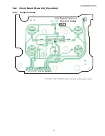
Page 91: ...peration 14 2 1 Component View ERASE STOP KEYS_E KEYS_C KEYS_B MEG_LED KEYIN2 KEYS_D KEYIN3 KEYIN1 ANS_LED 2APVCC ANS1 LOCAT INT A DOWN LED902 LED901 SKIP MSG2 MSG1 RPT UP KX TG6421 6431H PNLB1090Z PbF KX TG6421 CIRCUIT BOARD Base Unit_Operation Component View ...

Page 92: ...92 KX TG6421HGT KX TGA641FXT Memo ...

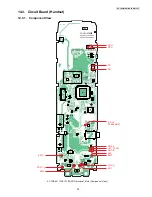
Page 93: ...801 R805 R802 R203 R208 R209 R310 R309 R308 R63 R225 R252 R251 R64 R330 R40 R331 R41 R42 R248 R249 R301 R305 R302 R303 R300 R304 R2 R73 R311 R30 R74 R31 R7 R6 R4 R45 L804 L4 L8 L5 RA2 RA4 RA61 D22 D21 D13 D14 D1 D7 D4 D3 Q11 Q12 Q9 C862 C105 C187 C186 C107 C106 C103 C104 C580 C175 C860 C182 C859 C36 C45 C820 C825 C861 C 8 0 8 C809 C810 C805 C806 C812 C827 L801 L803 C803 C819 C826 C822 TEST C46 C33...

Page 94: ... 2 Bottom View 1 SP R 2 5 UP DOWN S1 TALK SOFT_C SOFT_B SOFT_A 3 4 6 7 MIC 8 9 LED5 LED1 LED2 LED3 LED9 LED7 LED4 LED12 LED8 LED6 0 KX TGA641 CIRCUIT BOARD Handset_Main Bottom View CN5 A PbF PNLB1103Z KX TGA641 EUDECT KX TGA106 USDECT ...

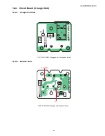
Page 95: ...Charger Unit 14 4 1 Component View 14 4 2 Bottom View J1 R1 D1 A PQUP11532Z PbF PQLV30055 PQLV30056 CIRCUIT BOARD Charger unit Component View TP4 TP3 1 2 J1 D1 A F1 PbF PQLV30055 PQLV30056 PQUP11532Z CIRCUIT BOARD Charger unit Bottom View TP4 GND TP3 ...

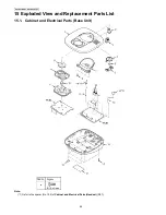
Page 96: ...96 KX TG6421HGT KX TGA641FXT 15 Exploded View and Replacement Parts List 15 1 Cabinet and Electrical Parts Base Unit Note 1 Refer to the spacer No 109 of Cabinet and Electrical Parts Handset P 97 ...

Page 97: ... Parts Handset Note 1 This cable is fixed by welding Refer to How to Replace the Handset LCD P 59 2 The rechargeable Ni MH battery P03P or HHR 4MRE is available through sales route of Panasonic 3 Attach the spacer No 122 to the exact location described above ...

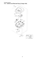
Page 98: ...98 KX TG6421HGT KX TGA641FXT 15 3 Cabinet and Electrical Parts Charger Unit ...

Page 99: ...99 KX TG6421HGT KX TGA641FXT 15 4 Accessories and Packing Materials 15 4 1 KX TG6421HGT ...

Page 100: ...100 KX TG6421HGT KX TGA641FXT 15 4 2 KX TGA641FXT ...

Page 101: ... MODULAR 4 L0AD02A00026 SPEAKER 5 PQHG10729Z RUBBER PARTS SPEAKER 6 PQHR11313Z GUIDE SPEAKER ABS HB 7 PNKE1030Z1 CASE CHARGE TERMINAL PS HB 8 PNBC1002Z2 BUTTON NAVIGATOR KEY ABS HB 9 PNHR1001Z GUIDE BUTTON PS HB 10 PNBC1001Z2 BUTTON MESSAGE AS HB 11 PNJK1045Y KEYBOARD SWITCH 12 PNJT1025Z CHARGE TERMINAL 13 PNLA1002Z ANTENNA 14 PNYE1009Z SPACER ANTENNA 15 PNKF1055Z1 CABINET COVER PS HB 16 PQHA10023...

Page 102: ...No Part No Part Name Description Remarks C22 PQCUV1A105KB 1 C23 ECJ0EB0J224K 0 22 S C25 ECUE1C103KBQ 0 01 C27 F2A1H100B132 10 C29 F1G1H5R0A480 5p C30 F1G1H5R0A480 5p C31 PQCUV1A225KB 2 2 C32 F2A1C1010119 100 C36 F2A1A3310040 330 C37 F1G1H5R0A480 5p C51 ECUE1A104KBQ 0 1 C52 ECUE1H221JCQ 220p C53 ECUE1H221JCQ 220p C54 ECUE1C223KBQ 0 022 C55 ECUE1A683KBQ 0 068 C56 ECUV1C104KBV 0 1 C60 ECUE1A104KBQ 0 ...

Page 103: ... CUSHION LCD 110 PNBC1265Z1 BUTTON VOLUME KEY ABS HB 111 PNJK1050Z KEYBOARD SWITCH 112 PNHX1165Z COVER LCD SHEET 113 PNJT1027Z CHARGE TERMINAL L 114 PNJT1026Z CHARGE TERMINAL R 115 PQHR11315Z GUIDE SPEAKER HOLDER ABS HB 116 L0AA02A00095 SPEAKER 117 PQHS10784Y SPACER SPEAKER NET 118 PQJC10056X BATTERY TERMINAL 119 PNKF1057Z1 CABINET COVER ABS HB 120 PQQT23182Z LABEL ATTENTION 121 PNGT2120Z NAME PLA...

Page 104: ...97 ECUE1H100DCQ 10p C103 ECUE1H101JCQ 100p Safety Ref No Part No Part Name Description Remarks C104 ECUE1H100DCQ 10p C105 ECUE1H101JCQ 100p C113 ECUE1H100DCQ 10p C138 ECUE1H100DCQ 10p C139 ECUE1H100DCQ 10p C147 ECUV1C105KBV 1 C152 ECUE1H102KBQ 0 001 C172 ECUV1C104KBV 0 1 C175 ECUV1C105KBV 1 C182 F1G1H3R0A480 3p C186 F1G1H2R0A480 2 0p C187 F1G1H2R0A480 2 0p C188 ECUE0J105KBQ 1 C331 ECUE0J105KBQ 1 C...

Page 105: ...FUSE Safety Ref No Part No Part Name Description Remarks A1 PQLV219CEX AC ADAPTOR A2 PQJA10075Z CORD TELEPHONE A3 PNQX1676Z INSTRUCTION BOOK 1 A4 PNQW1524Z LEAFLET QUICK GUIDE P1 PQPP10152Z PROTECTION COVER for Base Unit P2 XZB08X25B02 PROTECTION COVER for Handset P3 PNPK2266Z GIFT BOX Safety Ref No Part No Part Name Description Remarks A101 PQLV219CEX AC ADAPTOR A102 PNQX1700Z INSTRUCTION BOOK fo...

Reviews: