Panasonic KX-TG2511FXM, Service Manual
The Panasonic KX-TG2511FXM is a versatile phone system, featuring advanced call management settings and a high-quality build. Ensure its full potential with a free Service Manual, available for download at manualshive.com. This comprehensive manual provides step-by-step instructions and troubleshooting tips to optimize your user experience.
Share
Download


Reviews:
No comments
Related manuals for KX-TG2511FXM
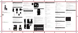
28512
Brand: GE Pages: 2
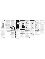
28310
Brand: GE Pages: 2
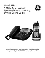
25982EE2
Brand: GE Pages: 100
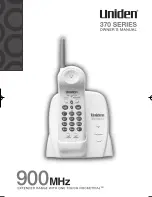
900 MHz
Brand: Uniden Pages: 12
OpenStage 15
Brand: Unify Pages: 19

NBX
Brand: 3Com Pages: 2

NBX 100
Brand: 3Com Pages: 57

3101
Brand: 3Com Pages: 2

356347_2004
Brand: Parkside Pages: 73

2.4 GHz Digital Spread Spectrum Cordless Telephone with Call Waiting/Caller ID
Brand: Radio Shack Pages: 16

TEL 30B
Brand: AUDIOLINE Pages: 12

Sigma 110 Voice Dou
Brand: Alcatel Pages: 2

LS6475-2
Brand: VTech Pages: 2

myPhone Jazz 202112
Brand: mPTech Pages: 65

Cordless Reciprocating Saw
Brand: Porter-Cable Pages: 25

BEOCOM 5
Brand: Bang & Olufsen Pages: 76

HOB-331-F
Brand: CEECO Pages: 15

HT-ATLAS
Brand: Hall Technologies Pages: 30


