7
KX-TG2511CA/KX-TG2512CA/KX-TGA250RU
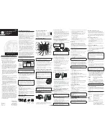
4 Technical Descriptions
4.1.
Block Diagram (Base Unit)
Analog
Front
End
T
o TEL_LINE
Bridge
Rect
D3D3
Hook Switch
Q4,Q5
Audio
Bell/Caller ID
Interface
CPU
18
16
23
20
21
19
24
BELL
HOOK
Off-Hook Line Voltage
25
A/D
D/A
ADPCM
Codec Filter
DSP
Speech Encoding
Speech Decoding
BMC
Burst Encoding
Burst Decoding
RF
PLL
5
3
77
75
9
10
EEPROM
SCL
SDA
57
58
44
Charge
Detector
(Optional)
BBIC
IC401
IC7
KX-TG2511/2512 BLOCK DIAGRAM
(BASE UNIT)
MOD/DEMOD
Charge
Pump
43
2.5V
X
T
A
L
X
1
X1
10.3
68
M
H
z
IC
801
R
X
n
R
X
p
T
X
p
T
X
n
P
on
P
S
E
L
V
DD
-P
A
D
R
V
4
3
6
7
T
X
on
R
X
on
D
801
6
72
AN
T1
AN
T2
9
8
AN
T1
ANT2
R
F
P
A
ANT1
AN
T2
78
73
74
80
L1
L
2
2
To AC Adaptor
Limit
Resistor
CHARGE
CONTACT
IC2
Q9
Q8
2.4V
Reg.
1.8V
Reg.
3.0 V
2.4 V
1.8 V
D
C
P
D
C
M
IC3
Summary of Contents for KX-TG2511CAM
Page 2: ...2 KX TG2511CA KX TG2512CA KX TGA250RU ...
Page 14: ...14 KX TG2511CA KX TG2512CA KX TGA250RU 4 6 Signal Route ...
Page 16: ...16 KX TG2511CA KX TG2512CA KX TGA250RU 8 Service Mode 8 1 Engineering Mode 8 1 1 Base Unit ...
Page 18: ...18 KX TG2511CA KX TG2512CA KX TGA250RU 8 1 2 Handset ...
Page 27: ...27 KX TG2511CA KX TG2512CA KX TGA250RU Cross Reference Check Point Base Unit P 35 ...
Page 29: ...29 KX TG2511CA KX TG2512CA KX TGA250RU Cross Reference Check Point Handset P 39 ...
Page 44: ...44 KX TG2511CA KX TG2512CA KX TGA250RU 10 1 2 Handset ...
Page 45: ...45 KX TG2511CA KX TG2512CA KX TGA250RU 10 1 3 Charger Unit ...
Page 77: ...77 KX TG2511CA KX TG2512CA KX TGA250RU 15 4 Accessories A2 A1 ...