background image

ORDER NO. KM40308169C8

Telephone Equipment

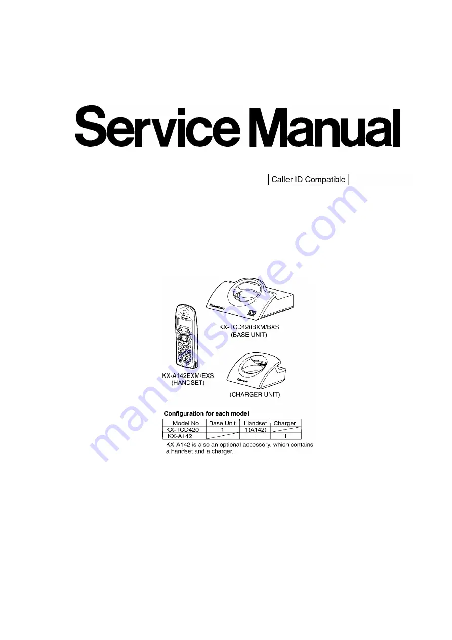
KX-TCD420BXM / KX-A142EXM / KX-TCD420BXS / KX-

A142EXS

Digital Cordless Answering System

Metalic Gray Version

Silver Version

(for Asia, Eastern Europe and Other areas)

SPECIFICATIONS

1

www.freeservicemanuals.info

1/2/2015

Digitized in Heiloo, Holland

Summary of Contents for KX-A142EXM

Page 1: ...t KX TCD420BXM KX A142EXM KX TCD420BXS KX A142EXS Digital Cordless Answering System Metalic Gray Version Silver Version for Asia Eastern Europe and Other areas SPECIFICATIONS 1 www freeservicemanuals info 1 2 2015 Digitized in Heiloo Holland ...

Page 2: ... in our manufacturing process which is made from Tin Sn Silver Ag and Copper Cu This model and others like it manufactured using lead free solder will have PbF stamped on the PCB For service and repair work we suggest using the same type of solder although with some precautions standard Pb solder can also be used Caution PbF solder has a melting point that is 50 F 70 F 30 C 40 C higher than Pb sol...

Page 3: ...y flow onto the opposite side See the figure below 1 1 Suggested PbF Solder There are several types of PbF solder available commercially While this product is manufactured using Tin Silver and Copper Sn Ag Cu you can also use Tin and Copper Sn Cu or Tin Zinc and Bismuth Sn Zn Bi Please check the manufac turer s specific instructions for the melting points of their products and any precautions for ...

Page 4: ...ll help prevent recurring malfunctions 1 Cover the plastic parts boxes with aluminum foil 2 Ground the soldering irons 3 Use a conductive mat on the worktable 4 Do not touch IC or LSI pins with bare fingers 3 CAUTION Danger of explosion if battery is incorrectly replaced Replace only with the same or equivalent type recommendenced by the manufacturer Dispose of used batteries according to the manu...

Page 5: ...ch power is off will be turned on automatically when it is placed on the base unit In normal use the handset and the base unit should be powered on at all times Note for Service The battery strength may not be indicated correctly if the battery is disconnected and connected again even after it is fully charged In that case by recharging the battery as mentioned above you will get a correct indicat...

Page 6: ...d If battery life is shortened then please check that battery and charge terminals are clean For maximum battery life it is recommended that the handset is not recharged until battery icon flashes 4 4 Replacing the Batteries If the icon flashes after a few telephone calls even when the handset batteries have been fully charged 2 batteries must be replaced Charge new batteries for approximately 7 h...

Page 7: ...e battery electrolyte Please use only Panasonic P03P Ni MH or P03H Ni Cd batteries Note for Service When Ni Cd batteries are fitted with the setting in icon might disappear and stop charging even if the handset is on the cradle for avoiding overcharge 5 LOCATION OF CONTROLS 5 1 Base Unit 5 2 Handset 7 www freeservicemanuals info 1 2 2015 Digitized in Heiloo Holland ...

Page 8: ...main connected at all times It is normal for the adaptor to feel warm during use Never install telephone wiring during a lightning storm The unit will not work during a power failure we recommend you connect a standard telephone on the same line for power protection 8 www freeservicemanuals info 1 2 2015 Digitized in Heiloo Holland ...

Page 9: ...aptor must remain connected at all times It is normal for the adaptor to feel warm during use 6 2 Symbols Used in This Service Manual 6 3 PIN Code 6 3 1 Base Unit 9 www freeservicemanuals info 1 2 2015 Digitized in Heiloo Holland ...

Page 10: ... will be able to enter new PIN As for the case that Base Unit and Handset are not linked with refer to Reset Base Unit PIN to Default 0000 When There is NO Handset Registered 6 3 2 Handset To exit the operation press any time For Service Hint 10 www freeservicemanuals info 1 2 2015 Digitized in Heiloo Holland ...

Page 11: ...original handset has broken and customer purchased a new one if customer forget base PIN customer cannot register the new handset and may ask to reset the PIN 6 3 3 3 Remedy Preparation Refer to JIGs and PC Connection 1 Solder a pin or lead wire to GND SDA and SCLK on base PCB 2 Plug in AC adaptor to the base 3 Turn on the power to the JIG 9V 4 Then connect the cable to each pins using clip As for...

Page 12: ...ks selectable options Ringer Mode All Handsets All Handsets Specific Handset No Number of Rings 3 Up to 6 rings Flash Earth Flash Flash Earth Flash Timing 600 msec 600 100 300 msec Pause Timing 3 seconds 3 seconds 5 seconds Call Restricted Handsets All Clear Each Handset can be set indivisually Call Restriction Numbers All Clear Up to 10 numbers up to 8 digits 4 Digit Base Unit PIN 0000 Dialling M...

Page 13: ...terns Key Tone ON ON OFF Call Waiting Tone ON ON OFF Range Warning Alarm OFF OFF ON Battery Low Alarm ON ON OFF Standby Mode Display Clock Clock OFF Base No Handset No Talk Mode Display Talk Time Talk Time Phone No Display Language English 10 languages Call BAR OFF OFF ON Direct Call Mode OFF OFF ON Direct Call Number Clear Up to 24 digits 4 Digit Handset PIN 0000 Auto Talk OFF OFF ON Base Unit Ac...

Page 14: ...to a PBX pressing RECALL allows you to access some features of your host PBX such as transferring an extension call 6 7 Dialling Pause for PBX line long distance service users A dialling pause is used when a pause in the dialling of the phone number is necessary using a PBX or accessing a long distance service For example when 9 line access number is dialled followed by a pause to access an outsid...

Page 15: ...assign up to 10 call restriction numbers up to 8 digits If you dial a restricted number the call does not connect and restricted number flashes To exit the operation press any time 1 The factory preset is 0000 2 The selected handset number flashes 6 9 Cancelling Call Restricted Handset s 15 www freeservicemanuals info 1 2 2015 Digitized in Heiloo Holland ...

Page 16: ...Off You cannot make any dialling if Call BAR is on When call BAR is on emergency calls cannot be made until Call BAR is cancelled To exit the operation press any time 1 The factory preset is 0000 2 If is selected is displayed Refer to Handset Display 6 11 Selecting the Display Language 16 www freeservicemanuals info 1 2 2015 Digitized in Heiloo Holland ...

Page 17: ... the dialling mode to tone or pulse depending upon your network service If you have a touch tone service select tone If you have rotary or pulse service select pulse To exit the operation press any time 1 The factory preset is 0000 6 13 Selecting Flash Earth Mode An earth relay can be installed as an option depending on your PBX requirements Please consult your nearest Panasonic Service Centre for...

Page 18: ...le Functions You can select and execute the following functions by pressing direct command as follows without programming These operations need to be done with the Handset near the base unit Press Press or until the arrow points to then press is displayed 1 18 www freeservicemanuals info 1 2 2015 Digitized in Heiloo Holland ...

Page 19: ...not pressed over 60 seconds the display will return to Setting Base 2 Refer to PIN Code for more details 7 DISPLAY 7 1 Handset Display For Service Hint 19 www freeservicemanuals info 1 2 2015 Digitized in Heiloo Holland ...

Page 20: ...rking telephone in its place If the known working telephone still has problems then please contact the customer service department of your Network provider If it operates correctly then the problem is likely to be a fault in your apparatus In this case contact your supplier for advice Your Network provider may charge you if they attend a service call that is not due to apparatus supplied by them T...

Page 21: ...21 www freeservicemanuals info 1 2 2015 Digitized in Heiloo Holland ...

Page 22: ...blank 8 2 Making a Call 1 If you need correction press CLEAR Digit is cleared to the left then enter numbers 8 3 Answering a Call Each ringer will start ringing with lower volume then gradually increase the volume when receiving a call 1 You can also answer a call by pressing any dialling button INTERCOM or 8 4 Setting the Clock Date 22 www freeservicemanuals info 1 2 2015 Digitized in Heiloo Holl...

Page 23: ...tion in the phonebook If you received a call from the same phone number you stored with a name in the phonebook the display will show the caller s name 8 5 1 Storing a Caller Information To exit the operation press any time 1 If you need correction press RIGHT or LEFT to move cursor then clear a character by pressing CLEAR and or enter characters Characters are cleared or added to the left of the ...

Page 24: ...character To enter characters see Character Selection below 2 To continue storing another caller information repeat the steps from 3 24 www freeservicemanuals info 1 2 2015 Digitized in Heiloo Holland ...

Page 25: ...e left of the flashing character If you need to clear or add more than one character repeat the steps from 7 5 To continue clearing another caller information repeat the steps from 2 8 5 2 Storing the Phone Number into the Phonebook When Pre dialling To exit the operation press any time 1 If you need correction press CLEAR Digit is cleared to the left then enter numbers 8 5 3 Storing the Number fr...

Page 26: ... flashing digit 8 5 4 Hot Key Speed Dial You can assign the dialling buttons 1 through 9 as hot keys You can choose 9 phone numbers from the phonebook To exit the operation press any time 1 If there is no item stored in the phonebook the display shows 2 The number is flashing if the dialling button is already assigned as a hot key 3 Phonebook registration will be remained even hot key registration...

Page 27: ...SEMBLY INSTRUCTIONS 9 1 Base Unit Shown in Fig To Remove Remove 1 Lower Cabinet Screws 2 6 12 A 2 2 Main P C Board Main P C Board 9 2 Handset 27 www freeservicemanuals info 1 2 2015 Digitized in Heiloo Holland ...

Page 28: ...ve Remove 3 Rear Cabinet Screws 2 10 B 2 4 Rear Cabinet Follow the procedure 5 Main P C Board Screw 2 8 C 1 Screws 2 8 D 2 Main P C Board 9 3 Charger Unit 28 www freeservicemanuals info 1 2 2015 Digitized in Heiloo Holland ...

Page 29: ...wer Cabinet Screws 2 6 14 E 2 7 Main P C Board Main P C Board 10 ASSEMBLY INSTRUCTIONS 10 1 Warning When Constructing the Base Unit 11 TROUBLESHOOTING GUIDE Flow Chart 29 www freeservicemanuals info 1 2 2015 Digitized in Heiloo Holland ...

Page 30: ...Link Check Handset Transmission Check Handset Reception SIGNAL ROUTE TAM Voice Prompt Problems 11 1 Check Power 11 1 1 Base Unit Is the AC Adaptor inserted into AC outlet Check AC Adaptor s specification 30 www freeservicemanuals info 1 2 2015 Digitized in Heiloo Holland ...

Page 31: ...ote BBIC is IC8 11 1 2 Handset Cross Reference Power Supply Circuit Reset Circuit Note BBIC is IC1 11 2 Check Battery Charge 11 2 1 Base Unit Cross Reference Charge Circuit 31 www freeservicemanuals info 1 2 2015 Digitized in Heiloo Holland ...

Page 32: ...Cross Reference Check Power Charge Circuit Note BBIC is IC1 11 2 3 Charger Unit Cross Reference Power Supply Circuit 11 3 Check Link 11 3 1 Base Unit 32 www freeservicemanuals info 1 2 2015 Digitized in Heiloo Holland ...

Page 33: ...Cross Reference Power Supply Circuit Adjustment Base Unit 11 3 2 Handset Cross Reference Power Supply Circuit 33 www freeservicemanuals info 1 2 2015 Digitized in Heiloo Holland ...

Page 34: ...nce SIGNAL ROUTE 11 5 Check Handset Reception Cross Reference HOW TO CHECK THE HANDSET SPEAKER SIGNAL ROUTE 11 6 Check Caller ID Cross Reference SIGNAL ROUTE 11 7 TAM Voice Prompt Problems 34 www freeservicemanuals info 1 2 2015 Digitized in Heiloo Holland ...

Page 35: ... Check Handset Reception EEPROM LAYOUT BASE UNIT TAM Voice Prompt Download 11 8 Bell Reception 11 8 1 Base Unit Note BBIC is IC8 11 8 2 Handset Cross Reference 35 www freeservicemanuals info 1 2 2015 Digitized in Heiloo Holland ...

Page 36: ...131A is recommended DC power it must be able to output at least 1A current under 9V Digital multi meter DMM it must be able to measure voltage and current Oscilloscope 12 1 2 JIGs and PC EEPROM serial JIGs 1 I2C PCB PQZZTCD705BX 2 RS232C cable PQZZ1CD705BX 3 Clip cable PQZZ2CD705BX 4 DC cable PQZZ3CD705BX PC which runs in DOS mode Batch file for setting PQZZTCD420BX 12 2 PC Setting 12 2 1 Connecti...

Page 37: ...written setfreq adjust Frequency of RFIC Type setfreq nn nn hookoff off hook mode on Base Type hookoff hookon on hook mode on Base Type hookon Getchk Read checksum Type getchk Wreeprom write eeprom Type wreeprom 01 23 45 01 23 is address and 45 is data to be written InitBsPIN bat Initial Base PIN to 0000 Type initBsPIN 12 3 TAM Voice Prompt Download 1 Connect the parallel cable from the VOICE PROM...

Page 38: ...rent Oscilloscope 13 1 2 JIGs and PC EEPROM serial JIGs 1 I2C PCB PQZZTCD705BX 2 RS232C cable PQZZ1CD705BX 3 Clip cable PQZZ2CD705BX 4 DC cable PQZZ3CD705BX PC which runs in DOS mode Batch file for PC setting PQZZTCD420BX 13 2 PC Setting 13 2 1 Connections 13 2 2 PC Setting 1 Open a window of MS DOS mode from the start up menu 2 Change a directory to the one with RTX_COM contained 3 Type SET RTX_C...

Page 39: ... unit does not respond to a call from handset Make adjustments in item A F M The base unit does not transmit or the transmit frequency is off Make adjustments in item A E H J L The transmit frequency is off Make confirmation in item A E H J L The transmit power output is low and the operating distance between base unit and handset is less than normal Make confirmation in item H K The reception sen...

Page 40: ...R74 D9 R71 Q12 D BBIC Confirmation 1 BBIC Confirmation Execute the command getchk 2 Confirm the returned checksum value Connection of checksum value and program number is shown below IC8 C53 C5 C55 C56 X1 R78 E BBIC Clock Adjustment TP15 1 Execute the command deactmac 2 Execute the command conttx 3 Input Command rdeeprom_00_00_02 then you can confirm the current value 4 Adjust the frequency of TP1...

Page 41: ...and hookoff and dtmf_up 3 Confirm that the high frequency 1477 06Hz group is 6dBm 2dBm 4 Execute the command dtmf_lo 5 Confirm that the low frequency 852 05Hz group is 8dBm 2dBm IC8 R55 C3 R30 C88 C1 R26 R25 Q9 R24 R27 C1 R20 H Transmitted Power Confirmation Remove the Antenna before starting step from 1 to 4 1 Configure the DECT tester CMD60 as follows Setting Test mode FP Traffic Channel 5 Traff...

Page 42: ...8 C7 C68 C69 R7 R80 C63 C6 R83 R84 C6 L3 C79 C67 C66 D10 C6 J Frequency Offset Confirmation Follow steps 1 to 3 of H above 4 Confirm that the frequency offset is 40kHz IC6 IC4 L2 C57 C61 C7 C77 C78 C7 C68 C69 R7 R80 C63 C6 R83 R84 C6 L3 C79 C67 C66 D10 C6 K Sensitivity Receiver Confirmation Follow steps 1 to 3 of H above 4 Set DECT tester power to 88dBm 5 Confirm that the BER is 1000ppm IC6 IC4 L2...

Page 43: ...77 C78 C7 C68 C69 R7 R80 C63 C6 R83 R84 C6 L3 C79 C67 C66 D10 C6 M RSSI Level Confirmation Follow steps 1 to 3 of H above 4 Set DECT tester power to 88dBm 5 Execute the command readrssi 6 Confirm 29 returned value 3E hex IC6 IC4 L2 C57 C61 C7 C77 C78 C7 C68 C69 R7 R80 C63 C6 R83 R84 C6 L3 C79 C67 C66 D10 C6 43 www freeservicemanuals info 1 2 2015 Digitized in Heiloo Holland ...

Page 44: ...mulator 9 Input audio signal 200mVrms 1kHz tone to Tel simulator DECT tester setting Scramble On AF Gen to ADPCM Off AF Meter Input ADPCM AF Gen Frequency 1000Hz AF Gen Level 200mVrms 10 Confirm hearing tone 300mVrms 100mVrms 11 Adjust audio level if required Make sure current value using getmicgain And then execute the command setmicgain xx where xx is the value 12 Confirm that the B field audio ...

Page 45: ...o level if required Make sure current value using getspkrgain And then execute the command setspkrgain xx where xx is the value 11 Confirm that the audio distortion at 600R of Tel simulator is 5 IC6 IC4 L2 C57 C61 C7 C77 C78 C7 C68 C69 R7 R80 C63 C6 R83 R84 C6 L3 C79 C67 C66 D10 C6 R20 C14 D7 R21 R22 R2 R85 C15 C3 R51 C92 R5 C32 Q2 R12 R13 Q4 R14 R15 D6 C6 C7 JMP9 P Charging Check 1 Connect Charge...

Page 46: ... across the regigster is 2 7V 0 2V D1 R1 R2 Note After the measuring sock up the solder of TP The connection of adjustment equipment are as shown in Adjustment Standard Charger Unit 14 4 Adjustment Standard Charger Unit When connecting the Simulator Equipments for checking please refer to below 14 4 1 Flow Solder Side View Note A is refered to ADJUSTMENTS BASE UNIT AND CHARGER UNIT 15 ADJUSTMENTS ...

Page 47: ... of base unit is low with noise Make confirmation in item L Does not link between base unit and handset Make confirmation in item A C H N The reception level is high or low Make adjustments in item O The transmit level is high or low Make adjustments in item P Refer to Adjustment 15 1 Adjustment Please follow the items below when BBIC or EEPROM are replaced Items Adjustment Point Procedure Check R...

Page 48: ...C1 X1 C16 C17 D Charge Control Check Charge Current Monitor Confirmation 1 Apply 6V between TP5 and TP6 with current limit of PSU to 200mA 2 Confirm that the charge current is ON OFF 3 SW to decrease current limit of PSU to 100mA 4 Confirm that the charge current is stable IC1 D4 L4 L5 Q2 Q3 R6 D2 R22 C26 F1 R21 R4 C33 E Charge Detection OFF Confirmation 1 Stop supplying 6V to TP5 and TP6 2 Execut...

Page 49: ... D6 D7 H BBIC Clock Adjusment TP19 1 Execute the command conttx 2 Adjust the frequency of TP19 executing thecommand setfreq 00 xx where xx is the value so that the reading of the frequency counter is 10 368000MHz 3Hz IC1 L3 C57 IC3 X1 C16 C17 I Transmitted Power Confirmation TP15 Remove the Antenna before starting step from 1 to 5 1 Configure the DECT tester CMD60 as follows Setting Test mode PP R...

Page 50: ... is the value IC1 IC3 C54 C66 C60 L3 C57 C55 C5 C62 R23 R2 C63 C64 C6 R18 K Frequency Offset Confirmation Follow steps 1 to 4 of I above 5 Confirm that the frequency offset is 50kHz IC1 IC3 C54 C66 C60 L3 C57 C55 C5 C62 R23 R2 C63 C64 C6 R18 L Sensitivity Receiver Confirmation Follow steps 1 to 4 of I above 5 Set DECT tester power to 88dBm 6 Confirm that the BER is 1000ppm IC1 IC3 C54 C66 C60 L3 C...

Page 51: ...P Mode Nomal RFPI 0102030405 2 Execute the command testmode 3 Execute the command regcmd60 4 Initiate connection from DECT tester 5 Execute the command openaudio 6 Confirm that the value of EEPROM address F3F is 02 If the value is not 02 by User set 02 and power off and power on and return to clause 2 7 Input audio signal 50mVrms 1kHz tone from DECT tester DECT tester setting Scramble On AF Gen to...

Page 52: ...at the audio distortion with DECT tester is 5 IC1 C8 R7 R8 C6 C7 C5 R5 R1 C4 IC3 C54 C66 C60 L3 C57 C55 C5 C62 R23 R2 C63 C64 C6 R18 Note After the measuring sock up the solder of TP PC Setting is required beforehand The connection of adjustment equipment are as shown in Adjustment Standard Handset 15 2 Adjustment Standard Handset When connecting the Simulator Equipments for checking please refer ...

Page 53: ...z 50 kHz Adjustment Base Unit K RX Sensitivity 1000 ppm Adjustment Base Unit L Timing Accuracy 10 ppm Adjustment Base Unit M RSSI Level 0x34 hex A hex Adjustment Base Unit N Refer to Adjustment 17 HOW TO CHECK THE HANDSET SPEAKER 1 Prepare the digital voltmeter and set the selector knob to ohm meter 2 Put the probes at the speaker terminals as shown below 53 www freeservicemanuals info 1 2 2015 Di...

Page 54: ...18 FREQUENCY TABLE MHz 54 www freeservicemanuals info 1 2 2015 Digitized in Heiloo Holland ...

Page 55: ... UNIT 20 CIRCUIT OPERATION BASE UNIT 20 1 Outline Base Unit consists of the following ICs as shown in BLOCK DIAGRAM BASE UNIT DECT BBIC Base Band IC IC6 Handling all the audio signal and data processing needed in a DECT base unit Controlling the DECT specific physical layer and radio section B urst Module Controller section ADPCM codec filter for speech encoding and speech decoding DSP section Ech...

Page 56: ...2 65V output Crystal Circuit 10 368MHz Charge Circuit Telephone Line Interface Circuit 20 2 Power Supply Circuit The power is supplied to the DECT BBIC RF Module EEPROM Relay Coil LED and Charge Contact from AC Adaptor 6V as shown in Fig 101 The power supply is as follows DECT BBIC IC8 J1 6V D4 IC2 IC3 IC8 IC6 IC7 RF Module IC9 J1 6V D4 IC2 IC9 EEPROM IC4 J1 6V D4 IC2 IC3 IC4 LED LED1 J1 6V D4 IC2...

Page 57: ...e Q2 is open to cut the DC loop current and decrease the ring load When ring voltage appears at the TP3 A and TP40 B leads when the telephone rings the signal is transferred as follows A C25 R40 R45 IC5 C28 R47 C29 R49 IC8 136 CLIP B C24 R39 R44 IC5 C28 R47 C29 R49 IC8 136 CLIP A C2 IC1 IC8 81 BELL B D2 D3 R1 IC1 IC8 81 BELlL ON OFF hook circuit 57 www freeservicemanuals info 1 2 2015 Digitized in...

Page 58: ...c Access P rofile standard DECT frame assigning to a time slot and channel etc In IC3 the carrier frequency is changing and frequency modulated RF signal is generated and amplified and radiated from antenna Handset detects the voice signal or data signal in the circuit same as the following explanation of Receiver Block 20 4 2 Receiver Block The signal of 1 152 MHz band 1 881792 MHz 1 897344 MHz w...

Page 59: ...rary operating parameters for RF etc Note Refer to EEPROM LAYOUT HANDSET 22 2 Power Supply Circuit Reset Circuit Circuit Operation When power on the Handset the voltage is as follows BATTERY 2 2 V 2 6V TP3 TP14 4V IC3 6 27 D3 IC1 37 IC1 39 63 2 65V The Reset signal generates R19 C23 and 2 65V 22 3 Charge Circuit Circuit Operation When charging the handset on the Base Unit the charge current is as ...

Page 60: ... Supply Circuit 22 4 Battery Low Power Down Detector Circuit Operation Battery Low and Power Down are detected by BBIC which check the voltage from battery The detected voltage is as follows Battery Low Battery voltage V Batt 2 3V The BBIC detects this level and starts flashing and battery alarm starts ringing Power Down Battery voltage V Batt 2 2V The BBIC detects this level and power down Note R...

Page 61: ...24 SIGNAL ROUTE 25 CPU DATA BASE UNIT 25 1 IC8 BBIC 61 www freeservicemanuals info 1 2 2015 Digitized in Heiloo Holland ...

Page 62: ...1 RXDB A 22 ANT1 DO ANT1 ON ANT1 OFF 23 VDD 24 VSS 25 ANT2 DO ANT2 ON ANT2 OFF 26 I2CLK DO Active Active 27 I2DAT DI O Data Data 28 VSS 29 CSROQ DO Read IC7 for Flash Memory 30 BSCL0 DO for Flash Memory 31 BSCL1 DO for Flash Memory 32 A0 DO for Flash Memory 33 A1 DO for Flash Memory 34 VDD 35 VSS 36 A2 DO for Flash Memory 37 A3 DO for Flash Memory 38 A4 DO for Flash Memory 39 A5 DO for Flash Memor...

Page 63: ...for Flash Memory 61 D7 DI O for Flash Memory 62 NO USE DO 63 P0 6 DO Make Break 64 NO USE DO 65 NO USE DO 66 VDD 67 VSS 68 NO USE DO 69 PULSE_CTRL DO Q7_ON Q7_OFF 70 P0 1 DO for Flash Memory 71 P0 0 DO No Key Key for Key 72 PX 2 DO Write IC4 for Flash Memory 73 PX 1 DO Read IC4 for Flash Memory 74 NO USE DO 75 NO USE DO 76 R1 DO LED ON LED OFF 77 NO USE DO 78 VDD 79 VSS 80 NO USE DO 81 TONE DI Rin...

Page 64: ...3 FRDY DO for Flash Memory 104 MD4 DO for Flash Memory 105 MD2 DO for Flash Memory 106 MD1 DI for Flash Memory 107 MD0 DO for Flash Memory 108 VDD 109 VSS 110 NO USE A 111 NO USE A 112 NO USE A 113 NO USE A 114 NO USE A 115 NO USE A 116 VSSA 117 VDDA 118 NO USE A 119 NO USE AI 120 NO USE AI 121 NO USE A 122 NO USE A 123 SON A 124 NO USE A 125 NO USE A 126 HOP A 127 HOPI A 128 NO USE A 129 REFVH A ...

Page 65: ...rks 1 LCD_SEGMENT D O Active 2 LCD_COMMON D O Active 3 VDD 4 VSS 5 LCD_COMMON D O Active 6 LCD_COMMON D O Active 7 LCD_COMMON D O Active 8 LCD_COMMON D O Active 9 LCD_COMMON D O Active 10 PA_SW D O PA ON 11 T R SW D O Transmit 12 RX_DATA D I Active 13 SYEN D O Active 14 SYDA D O Active 15 SYCL D O Active 16 TX_DATA A O Active 17 KEY_IN D I No Key 18 KEY_IN D I No Key 19 KEY_IN D I No Key 20 KEY_IN...

Page 66: ... 42 LSRP A O 43 BANDGAP_REF A O 44 MICS A O 45 MICP A I 46 MICN A I 47 Reference Voltage A O 48 RSSI A I 49 P0 4 D I 50 AD4N A I 51 AD4P A I 52 NO USE D I 53 KEY_STRB D O Active 54 KEY_STRB D O Active 55 KEY_STRB D O Active 56 LCD_SEGMENT D O Active 57 LCD_SEGMENT D O Active 58 LCD_SEGMENT D O Active 59 KEY_STRB D O Active 60 KEY_STRB D O Active 61 LCD_SEGMENT D O Active 62 LCD_SEGMENT D O Active ...

Page 67: ...SEGMENT D O Active 93 LCD_SEGMENT D O Active 94 LCD_SEGMENT D O Active 95 LCD_SEGMENT D O Active 96 LCD_SEGMENT D O Active 97 LCD_SEGMENT D O Active 98 LCD_SEGMENT D O Active 99 LCD_SEGMENT D O Active 100 LCD_SEGMENT D O Active 27 EEPROM LAYOUT BASE UNIT 27 1 Scope The purpose of this section is to describe the layout of the EEPROM IC4 for the KX TCD420 Base Unit The EEPROM contains hardware softw...

Page 68: ... eeprom default loader only if the location contains all 1 s byte 0xFF word FFFFh i e it has never been set EEPROM location which is not set at all Country Setting x Default no specific country setting so revert to default value 27 3 EEPROM Layout 27 3 1 General Setup Address Default Name Country Setting Type Description 0000 01 00 E0 EepromOscillator x A Frequency adjustment 0002 20 ModulationDev...

Page 69: ...UAK for hanset 4 for factory use 00D0 00DF UAK_5 x UAK for hanset 5 for factory use 00E0 00EF UAK_6 x UAK for hanset 6 for factory use 27 3 2 Switch Control Address Default Name Country Setting Type Description 09F1 00 HsRegInfo RegFlags x D Handset registration info registration ON OFF 1 reg 0 no reg 09F2 00 HsRegInfo EmcFlags x D Handset registration info EMC flags Bit 6 7 not used 0 5 handset 1...

Page 70: ...BreakTime 2 1E D Calibrated loop break time for short break Unit 10 ms defaultst to 700 ms 27 3 4 Clip Caller ID configuration Address Default Name Country Setting Type Description 0F1C 70 Detect x D CLIP detect configuration Bit 0 2 Mode 0 Learn mode 1 DTMF only 3 Generic mod 4 Russian CLIP only 3 Unused4 4 Onhook 1 enable 0 disable 5 Offhookk 1 enable 0 disable 6 Msgwaiting 1 enable 0 disable 7 ...

Page 71: ...KPN vmwi 1 enable 0 disable 8 ProtocolPriority If 2 mutual exclusive parameters occurs the 1st in the protocol message has priority 9 UseCallType Verify the Call Type parameter if available when receiving Call Back CLIP at busy subscriber 1 enable 0 disable 10 AddTop0IfNo0 Automatic addition of 0 if top of Caller ID is not 0 1 enable 0 disable 11 DtmfDigitsOnly Parse DTMF clip without start and or...

Page 72: ...y F Spain 13 South Africa 14 Russia 0F41 0F60 FF TamTagInfo x A Message TAG information Bit 0 3 Odd number MSG 4 7 Even number MSG 0 Reserve 1 2WayInfo 0 Not 2WayRec 1 2WayRecMsg 2 New Info 0 OLD 1 NEW 3 OGM Info Not used 4 Reserve 5 2WayInfo 0 Not 2WayRec 1 2WayRecMsg 6 ARSMultipleCarrierMenuEnabled enabled 7 OGM Info Not used 72 www freeservicemanuals info 1 2 2015 Digitized in Heiloo Holland ...

Page 73: ...on 0 Normal 1 7 DSC time selection 0 immediately 1 6sec 0F62 00 TamPrgRings x A Current number of rings for automatic answering Range 0 Auto 2 7 0F63 0F64 FF TamPrgRmtCode x A Current Remote code e g 123 Address 0x0F63 0xF1 Address 0x0F64 0x23 0F65 10 CountryData 18 D Each country data Bit 0 Reserve 1 Reserve 2 Max time in Line Remote Not Used 3 TimeData for voice prompt 0 24hour 12hour 4 VicMenuD...

Page 74: ... ON 3 Switching of VOX Sense ON OFF 0 OFF 1 ON 4 Key Click Tone ON OFF Not used 5 Select Compression Rate Menu 0 Not Active 1 Active 6 2 Way Beep interval2 For UK 15s per 400ms 1khz 2 wayBeepInterval 0 2wayBeepInterval2 0 For FR 20s per 160ms 1khz 2wayBeepInterval 1 2wayBaeepInterval2 0 For AL 15s per 420ms 1 4khz 2wayBeepInterval 1 2wayBeepInterval2 1 7 Reserve 0F68 00 TamPrgWordMode x D Language...

Page 75: ...figuration LSB Bits 1 enable 0 disable 0 FlashTime1Enabled enabled 1 FlashTime2Enabled enabled 2 FlashTime3Enabled enabled 3 KeyClicksEnable enabled 4 ARSCarrierMenuEnabled enabled 5 ARSIntDeletionMenuEnabled enabled 6 ARSMultipleCarrierMenuEnabled enabled 7 ARSMultipleAreaCodeMenuEnabled enabled 28 EEPROM LAYOUT HANDSET 28 1 Scope The purpose of this section is to describe layout of the EEPROM IC...

Page 76: ...M location is set during the production test and should not be overwritten The value is set by the eeprom default loader only if the location contains 0xFF i e it has never been set EEPROM location which is not set at all Country Setting x Default no specific country setting so revert to default value 28 3 EEPROM contents 28 3 1 General Setup Address Default Name Type Description 0000 0001 00 Eepr...

Page 77: ...TATUS_2 Status for registration 2 0147 0156 UAK_2 UAK for registration 2 0160 0164 RFPI_3 Base 3 RFPI for registration 3 0165 SerClass_3 Service class for registration 3 0166 LAL_3 Location area level for registration 3 0167 IPUI_LEN_3 IPUI length for registration 3 0168 0174 IPUI_3 IPUI for registration 3 0175 ZAP_3 ZAP for registration 3 0176 STATUS_3 status for registration 3 0177 0186 UAK_3 UA...

Page 78: ...rkish 06 Hungarian 07 Portuguese 08 Polish 09 Command 0A German 0469 07 MaxDigitsToMatch x D Valid values 01 FF Digits above this value will not be evaluated when matching 046A 05 MinDigitsToMatch x D Valid values 01 FF Must be lower than MaxDigitsToMatch If all digits of one of the numbers match completely with at least this number of digits we have a match Or if they match completely with less d...

Page 79: ...for volumestep 1 x D Bit7 AOG Bit6 AOG2 Bit5 bit0 Gain receive values ranging from 0x00 to 0x30 each step representing 1 dB 0F37 5F GR offset for volumestep 2 x A Bit7 AOG Bit6 AOG2 Bit5 bit0 Gain receive values ranging from 0x00 to 0x30 each step representing 1 dB 0F38 46 GR offset for volumestep 3 00 D Bit7 AOG Bit6 AOG2 Bit5 bit0 Gain receive offset to volumestep 2 values ranging from 0x00 0x30...

Page 80: ...nversation 29 HOW TO REPLACE FLAT PACKAGE IC 29 1 Preparation PbF Pb free Solder Soldering Iron Tip Temperature of 700 F 20 F 370 C 10 C Note We recommend a 30 to 40 Watt soldering iron An expert may be able to use a 60 to 80 Watt iron where someone with less experience could overheat and damage the PCB foil Flux Recommended Flux Specific Gravity 0 82 Type RMA lower residue non cleaning type Note ...

Page 81: ...p so that it flows under the pins as they are heated 29 3 Modification Procedure of Bridge 1 Add a small amount of solder to the bridged pins 2 With a hot iron use a sweeping motion along the flat part of the pin to draw the solder from between the adjacent pads 30 CABINET AND ELECTRICAL PARTS LOCATION BASE UNIT 81 www freeservicemanuals info 1 2 2015 Digitized in Heiloo Holland ...

Page 82: ...82 www freeservicemanuals info 1 2 2015 Digitized in Heiloo Holland ...

Page 83: ...31 CABINET AND ELECTRICAL PARTS LOCATION HANDSET 32 CABINET AND ELECTRICAL PARTS LOCATION CHARGER UNIT 83 www freeservicemanuals info 1 2 2015 Digitized in Heiloo Holland ...

Page 84: ...33 ACCESSORIES AND PACKING MATERIALS 84 www freeservicemanuals info 1 2 2015 Digitized in Heiloo Holland ...

Page 85: ...33 1 KX TCD420BXM BXS 33 2 KX A142EXM EXS 85 www freeservicemanuals info 1 2 2015 Digitized in Heiloo Holland ...

Page 86: ...34 TERMINAL GUIDE OF THE ICs TRANSISTORS AND DIODES 34 1 Base Unit 86 www freeservicemanuals info 1 2 2015 Digitized in Heiloo Holland ...

Page 87: ...this item After the discontinuation of this assembly in production the item will continue to be available for a specific period of time The retention period of availability is dependant on the type of assembly and in accordance with the laws governing part and product retention After the end of 87 www freeservicemanuals info 1 2 2015 Digitized in Heiloo Holland ...

Page 88: ...of some identical parts For that reason it may be different from the installed part 4 ISO code Example ABS 94HB of the remarks column shows quality of the material and a flame resisting grade about plastics 5 RESISTORS CAPACITORS Unless otherwise specified All resistors are in ohms K 1000 M 1000k All capacitors are in MICRO FARADS F P F Type Wattage of Resistor 35 1 Base Unit 35 1 1 Cabinet and El...

Page 89: ... with PQZZTCD420BX Ref No Part No Part Name Description Remarks PCB1 PQWP1D420BXH MAIN P C BOARD ASS Y RTL ICs IC2 PQVILM1117MP IC S IC3 PSVIXC62FP27 IC IC4 PQWI2D420BXH IC 1 IC5 PQVILMV321M5 IC IC6 PQWI3D420BXH IC 1 IC7 PQWI1D420BXH IC 1 IC8 C1CB00001558 IC TRANSISTORS Q2 2SA1625 TRANSISTOR SI S Q4 PQVTBF822T7 TRANSISTOR SI Q7 B1ABCE000009 TRANSISTOR SI Q8 B1ABCE000009 TRANSISTOR SI Q9 2SD1994A T...

Page 90: ...RJ3GEYJ474 470K R29 ERJ3GEYJ105 1M R30 ERJ3GEYJ221 220 R31 PQ4R18XJ100 10 S R32 ERJ3GEYJ103 10K R33 ERJ3GEYJ222 2 2K R34 ERJ3GEYJ151 150 R35 ERJ3GEYJ751 750 R36 ERJ3GEYJ103 10K R37 ERJ3GEYJ102 1K R38 ERJ3GEYJ102 1K R39 ERJ3GEYJ684 680K R40 ERJ3GEYJ684 680K R41 ERJ3GEYJ473 47K R42 ERJ3GEYJ124 120K R43 ERJ3GEYJ473 47K R44 ERJ3GEYJ101 100 R45 ERJ3GEYJ101 100 R46 ERJ3GEYJ124 120K R47 ERJ3GEYJ823 82K R...

Page 91: ...EYJ681 680 R86 ERJ3GEYJ155 1 5M C11 PQ4R10XJ562 5 6K S C42 ERJ3GEYJ472 4 7K C56 ERJ3GEY0R00 0 JMP9 PQ4R10XJ000 0 S CAPACITORS C1 ECUV1C104KBV 0 1 C2 ECQE2E474KZ 0 47 S C3 ECUV1H103KBV 0 01 C4 ECUV1H103KBV 0 01 C6 ECKD2H681KB 680P S C7 ECKD2H681KB 680P S C10 ECUV2H332KB 0 0033 C14 ECUV1H103KBV 0 01 C15 ECUV1H103KBV 0 01 C16 PQCUV1A105KB 1 C17 ECUV1H103KBV 0 01 C18 PQCUV1A105KB 1 C19 PQCUV1C104KB 0 ...

Page 92: ... 4 7 C62 ECUV1H060DCV 6P S C63 ECUV1H100DCV 10P C64 ECUV1H100DCV 10P C65 ECUV1H030CCV 3P C66 ECUV1H2R0CCV 2 C67 ECUV1H100DCV 10P C68 ECUV1H2R0CCV 2 C69 ECUV1A475KB 4 7 C70 ECUV1H102KBV 0 001 C71 ECUV1H101JCV 100P C72 ECUV1H102KBV 0 001 C75 ECUV1H100DCV 10P C76 ECUV1H100DCV 10P C77 PQCUV1H020CC 2P C78 ECUV1H2R0CCV 2 C79 ECUV1H100DCV 10P C80 ECUV1H2R0CCV 2 C88 ECUV1H100DCV 10P C89 ECUV1H220JCV 22P C...

Page 93: ...A00016 SPEAKER 109 PQSA10133Z ANTENNA 110 PQJT10204Z TERMINAL L 111 PQJT10205Z TERMINAL R 112 PQHX11202Z INSULATOR 113 PQJC10058Z BATTERY TERMINAL 114 PQJC10057Z BATTERY TERMINAL 115 PQJC10056Z BATTERY TERMINAL 116 PQKF10582Z5 CABINET COVER for KX A142EXM ABS HB 116 PQKF10582Z4 CABINET COVER for KX A142EXS ABS HB 117 PQGT15510Z NAME PLATE for KX A142EXM 117 PQGT15748Z NAME PLATE for KX A142EXS 118...

Page 94: ...COILS L2 G1A470L00001 COIL L3 PQLQR4D4R7K COIL L4 G1C100MA0072 COIL L5 G1C100MA0072 COIL F1 PQLQR2M5N6K COIL S RESISTORS R1 ERJ3GEYJ222 2 2K R2 ERJ8BQJR30 0 3 R3 ERJ3GEYJ560 56 R4 ERJ3GEYJ103 10K R5 ERJ3GEYJ331 330 R6 ERJ3GEYJ332 3 3K R7 ERJ3GEYJ331 330 R8 ERJ3GEYJ331 330 R11 ERJ3GEY0R00 0 R17 ERJ3GEY0R00 0 R18 ERJ3GEYJ330 33 R19 ERJ3GEYJ153 15K R20 ERJ3GEY0R00 0 R21 ERJ6RSJR10V 0 1 R22 ERJ3GEY0R0...

Page 95: ... X1 H0D103500002 CRYSTAL OSCILLATOR 35 3 Charger Unit 35 3 1 Cabinet and Electrical Parts Ref No Part No Part Name Description Remarks 1 PQLV30018ZM1 CHARGER for KX A142EXM 1 PQLV30018ZS1 CHARGER for KX A142EXS 1 1 PQGG10155Y5 GRILLE for KX A142EXM ABS HB 1 1 PQGG10155Y4 GRILLE for KX A142EXS ABS HB 1 2 PQKM10591Y3 CABINET BODY for KX A142EXM PS HB 1 2 PQKM10591Y2 CABINET BODY for KX A142EXS PS HB...

Page 96: ...P2 PQPP10084Z PROTECTION COVER for Handset P3 PQPK13967Z GIFT BOX 35 4 2 KX A142EXM EXS Ref No Part No Part Name Description Remarks A1 PQLV200CEZ AC ADAPTOR A2 PQQX13629Y INSTRUCTION BOOK A3 PQQW12846W LEAFLET RECHARGE P1 PQPP10086Z PROTECTION COVER for Charger Unit P2 PQPP10084Z PROTECTION COVER for Handset P3 PQPK13899Z GIFT BOX 35 5 Fixtures and Tools Part No Part Name Description Remarks PQZZ...

Page 97: ...nent View 39 2 Flow Solder Side View 40 CIRCUIT BOARD HANDSET 40 1 Component View 40 2 Flow Solder Side View 41 CIRCUIT BOARD CHARGER UNIT 41 1 Component View 41 2 Flow Solder Side View H M KXTCD420BXM KXA142EXM KXTCD420BXS KXA142EXS 97 www freeservicemanuals info 1 2 2015 Digitized in Heiloo Holland ...

Page 98: ...PbF IC7 IC8 IC9 144 109 108 1 1 16 17 32 1 11 36 35 28 18 73 72 Marked www freeservicemanuals info 1 2 2015 Digitized in Heiloo Holland ...

Page 99: ...PbF D1 J1 CIRCUIT BOARD CHARGER UNIT Component View www freeservicemanuals info 1 2 2015 Digitized in Heiloo Holland ...

Page 100: ...XM EXS CIRCUIT BOARD HANDSET Flow Solder Side View 1 PROG PbF BOOK UP POWER CAN DOWN RIGHT REDIAL LEFT 1 2 3 6 5 7 0 R 4 9 8 INT MIC TALK 36 CN2 www freeservicemanuals info 1 2 2015 Digitized in Heiloo Holland ...

Page 101: ...7 TP18 C20 C23 C18 L5 L4 R21 R6 C24 X1 Q1 C31 TP19 TP13 TP17 TP14 TP16 TP12 TP3 TP4 TP10 BAT GND SCL SDA C57 C64 C56 C55 11 18 1 28 27 26 25 24 23 22 21 20 19 18 28 2 3 4 5 6 7 8 9 10 11 12 13 14 15 16 17 34 33 32 31 30 29 1 IC3 C60 TP2 SP BBIC 41 TP1 SP BBIC 42 TP14 4V RF Clock BBIC 23 10 368 MHz VDD 2 65V CDT BBIC 27 TP12 CN3 TP3 GND TP4 KX A142EXM EXS CIRCUIT BOARD HANDSET Component View www fr...

Page 102: ...P15 TP8 TP7 TP11 TP106 TP9 TP1 2 4 1 5 6 TP4 TP2 TP3 TP10 TP6 TP5 B0 B4 B8 B1 GND MODE SCL SDA VDD J105 PbF J102 J104 J103 J101 B2 CHARGE CHARGE IC3 Output 2 8V CHARGE CHARGE IC2 Input 5 5V IC2 Output 4 0V RF Clock 10 368MHZ www freeservicemanuals info 1 2 2015 Digitized in Heiloo Holland ...

Page 103: ...R50 Q8 Q12 Q9 B C E R41 R43 R47 R57 R80 R64 R62 R57 R61 R83 R84 D10 R79 L3 Q3 Q4 Q7 Q5 Q11 Q13 Q10 Q6 Q2 R1 R42 R44 R3 C1 C28 CS 14 1 1 1 1 4 5 8 16 17 32 28 15 INT SDX SDR SCLK C26 C91 C44 C63 C84 C64 C34 C61 C54 C55 R86 C58 R82 C39 C45 L2 36 35 C72 C71 C60 C68 C80 C 6 6 C 6 2 C73 C79 C82 C81 C65 C74 ANT C6 C8 C3 C4 C9 C41 73 72 C40 C10 C7 C12 C70 C14 C19 C18 C23 C22 C16 C30 C29 C93 C92 C49 C89 R...

Page 104: ...TP3 R2 27 TP4 D1 2 1 J1 pinL DC_PLUG 22 Charge_minus TP1 TP2 R1 Charge_plus SCHEMATIC DIAGRAM CHARGER UNIT www freeservicemanuals info 1 2 2015 Digitized in Heiloo Holland ...

Page 105: ...64 K1 0 X1 TP13 C55 C2P C56 C2P C54 D10P TP17 TP16 C65 C2P C25 NC D5 NC C66 C2P TP15 IC3 5 RSSI 6 VCC_OC 7 GND 8 SYCL 9 SYDA 10 SYEN 11 GND 12 RXDSG 13 SYRI 14 GND 16 GND 17 GND 18 GND 19 GND 20 RXDA 21 GND 22 GND 23 GND 24 PAON 25 GND 26 GND 27 VCC_PA 28 GND 29 GND 30 GND 31 GND 32 GND 33 RF1 34 GND GND 1 GND 2 GND 3 TXDA 4 CN5 1 SP 2 SP D6 D7 TP19 R24 0 POWER SP 400µs typically 2 5V 0 5V 0V KX A...

Page 106: ... S20 S5 S3 S18 S25 S23 S15 S16 S4 S22 S21 S8 S9 C18 K0 1 C20 K0 1 C21 K0 1 C22 K0 1 C23 K0 1 C27 K0 1 R11 0 R21 0 1 F1 S24 S19 S14 S2 S1 CN2 1 C5 2 C4 3 C3 4 C2 5 C1 6 C0 7 S29 8 S28 9 S27 10 S26 11 S25 12 S24 13 S23 14 S22 15 S21 16 S20 17 S19 18 S18 19 S17 20 S16 21 S15 22 S14 23 S13 24 S12 25 S11 26 S10 27 S9 28 S8 29 S7 30 S6 31 S5 32 S4 33 S3 34 S2 35 S1 36 S0 TP10 TP8 TP12 TP7 S13 S6 R16 NC ...

Page 107: ...64 K1 0 X1 TP13 C55 C2P C56 C2P C54 D10P TP17 TP16 C65 C2P C25 NC D5 NC C66 C2P TP15 IC3 5 RSSI 6 VCC_OC 7 GND 8 SYCL 9 SYDA 10 SYEN 11 GND 12 RXDSG 13 SYRI 14 GND 16 GND 17 GND 18 GND 19 GND 20 RXDA 21 GND 22 GND 23 GND 24 PAON 25 GND 26 GND 27 VCC_PA 28 GND 29 GND 30 GND 31 GND 32 GND 33 RF1 34 GND GND 1 GND 2 GND 3 TXDA 4 CN5 1 SP 2 SP D6 D7 TP19 R24 0 POWER SP 400µs typically 2 5V 0 5V 0V KX A...

Page 108: ...R50 8 2K R49 C6P C54 J27P C55 K0 082 C47 J102 1 J103 1 J104 1 J101 1 J105 1 1K R72 1K R73 1K R71 100 R74 100K R54 100 R55 D10P C33 1K R77 10K R75 10K R76 2 8V K0 1 C48 68K R53 K0 033 C49 TP7 TP8 2 8V Q5 NC C12 NC NC C13 NC R18 NC R19 NC R16 R20 0 NC R17 Q7 1K R37 10K R36 2 8V Q8 1K R38 C56 0R00 R78 150K TP105 TP104 TP103 TP102 TP101 C50 Z1 0 C51 Z1 0 C52 Z1 0 D9 1 3 2 2 8V K0 015 C46 4 0V C60 J33P...

Page 109: ...C 10 NC 11 CS 12 SCK 13 SI 14 SO 15 NC 16 NC 17 NC 18 NC 19 NC 20 NC 21 NC 22 NC 23 NC 24 NC 25 NC 26 NC 27 NC 28 NC 2 VIN 3 VSS 1 VOUT 47K R41 47K R43 680K R39 100 R44 100 R45 K0 1 C28 82K R47 Q11 1K R48 C8 NC R8 NC R9 NC C9 NC JMP1 NC TP2 NC R58 33 R59 33 R60 TP5 2 8V K0 1 C44 10K R65 NC R7 4 0V NC D1 Q1 NC TP13 10K R64 2 8V 10K R63 2 8V RLY1 NC NC 1 2 3 4 7 8 9 10 NC JMP6 JMP8 NC JMP7 NC D4 4 7...

Page 110: ...R50 8 2K R49 C6P C54 J27P C55 K0 082 C47 J102 1 J103 1 J104 1 J101 1 J105 1 1K R72 1K R73 1K R71 100 R74 100K R54 100 R55 D10P C33 1K R77 10K R75 10K R76 2 8V K0 1 C48 68K R53 K0 033 C49 TP7 TP8 2 8V Q5 NC C12 NC NC C13 NC R18 NC R19 NC R16 R20 0 NC R17 Q7 1K R37 10K R36 2 8V Q8 1K R38 C56 0R00 R78 150K TP105 TP104 TP103 TP102 TP101 C50 Z1 0 C51 Z1 0 C52 Z1 0 D9 1 3 2 2 8V K0 015 C46 4 0V C60 J33P...

Page 111: ...HARGE CIRCUIT Q2 CHARGE CHARGE DETECT SWITCHED SUPPLY Q1 CHARGE CONTACTS TP5 4 0V VDDBAT VDDLR SWITCH 31 XTAL 10 368 MHz KEYPAD COLUMNS ROWS LCD 14 Seg Display ON SWITCH 38 27 26 36 37 28 2 5 9 COM 0 5 segment 0 29 1 87 EARPIECE 42 41 45 17 21 53 55 59 60 34 Burst Encoding Burst Decoding TP6 D3 X1 90 100 72 76 78 84 61 62 56 58 KX A142EXM EXS BLOCK DIAGRAM HANDSET www freeservicemanuals info 1 2 2...

Page 112: ...XDA J1 J2 IC8 IC9 4 0V Reg 2 65V Reg 4 0V 2 65V VUNREG 27 26 133 123 63 12 20 139 5 22 25 18 5 6 4 RF Module 20 5 10 33 7 5 XTAL 10 368 X1 MHz DTXAF 136 Bell Caller ID Interface ANT1 ANT2 to Tel_Line A B to AC Adaptor RING 81 Ring Det 76 Clip Der Flash IC7 D0 D7 A0 A17 PROM 30 ADDRES DATA CTRL 29 SCK 1 11 14 13 12 103 104 106 105 107 SI SO CS RD5 BUSY Serial Flash ROM IC6 71 Page Limit Register CH...

Page 113: ...27 TP18 C20 C23 C18 L5 L4 R21 R6 C24 X1 Q1 C31 TP19 TP13 TP17 TP14 TP16 TP12 TP3 TP4 TP10 BAT GND SCL SDA C57 C64 C56 C55 11 18 1 28 IC3 C60 DECT tester CMD60 I J K L M N O P Frequency Counter H Digital Volt Meter A Digital Volt Meter B C E F H I O P DC 6V Oscilloscope Current Probe D E D D TP5 TP6 TP7 TP8 DC 2 20V 2 40V F G To PC JIG AF SG DECT TESTER CMD60 AF Volt Meter DECT TESTER CMD60 www fre...

Page 114: ...PbF R1 R2 TP4 TP1 TP2 TP3 Digital Volt Meter 12Ω 2W A www freeservicemanuals info 1 2 2015 Digitized in Heiloo Holland ...

Page 115: ...E SCL SDA VDD J105 PbF J102 J104 J103 J101 B2 CHARGE CHARGE Digital Volt Meter A Digital Volt Meter B Frequency Counter E DTMF tester Tel Simulator F N O G Digital Volt Meter C P To PC JIG Digital Volt Meter D E F G H N O 12Ω 2W www freeservicemanuals info 1 2 2015 Digitized in Heiloo Holland ...

Page 116: ...C78 C33 C36 C87 C86 C37 C67 C76 C69 C83 C85 C96 C32 C94 R50 Q8 Q12 Q9 B C E R41 R43 R47 R57 R80 R64 R62 R57 R61 R83 R84 D10 R79 L3 Q3 Q4 Q7 Q5 Q11 Q13 Q10 Q6 Q2 R1 R42 R44 R3 C1 C28 CS 14 1 1 1 1 4 5 8 16 17 32 1 11 28 15 INT SDX SDR SCLK C26 C91 C44 C63 C84 C64 C34 C61 C54 C55 R86 C58 R82 C39 C45 L2 36 35 C72 C71 C60 C68 C80 C 6 6 C 6 2 C73 C79 C82 C81 C65 C74 28 18 ANT C6 C8 C3 C4 C9 C41 73 72 C...

Page 117: ...b by pulling black lead wire when opening the cabinet and turning the PCB over The terminal cannot have enough elastic force cannot have good contact with handset and it will result in charge problem OK NG Rib www freeservicemanuals info 1 2 2015 Digitized in Heiloo Holland ...

Page 118: ... C Copyright 1985 2000 Microsoft Corp C cd dect C DECT DOSKEY C DECT SET RTX_COM 1 C DECT initbspin C DECT call wreeprom bat 00 25 00 C DECT call wreeprom bat 00 26 00 C DECT _ www freeservicemanuals info 1 2 2015 Digitized in Heiloo Holland ...

Page 119: ...Clip G N D S D A S C L Base PCB J105 J102 J104 J103 J103 B1 GNDMODE SCL SDA VDD B2 www freeservicemanuals info 1 2 2015 Digitized in Heiloo Holland ...

Page 120: ...PbF D1 J1 Marked PbF R1 R2 TP4 TP1 TP2 TP3 Marked Component View Flow Solder Side View www freeservicemanuals info 1 2 2015 Digitized in Heiloo Holland ...

Page 121: ...Marked 1 PROG PbF BOOK UP POWER CAN DOWN RIGHT REDIAL LEFT 1 2 3 6 5 7 0 R 4 9 8 INT MIC TALK 36 CN2 www freeservicemanuals info 1 2 2015 Digitized in Heiloo Holland ...

Page 122: ...Marked PbF IC1 IC2 100 80 5 8 4 1 50 51 30 31 1 11 18 1 28 IC3 www freeservicemanuals info 1 2 2015 Digitized in Heiloo Holland ...

Page 123: ...3 TP15 TP8 TP7 TP11 TP106 TP9 TP1 2 4 1 5 6 TP4 TP2 TP3 TP10 TP6 TP5 B0 B4 B8 B1 GND MODE SCL SDA VDD J105 PbF J102 J104 J103 J101 B2 CHARGE CHARGE www freeservicemanuals info 1 2 2015 Digitized in Heiloo Holland ...

Page 124: ...PbF R1 R2 TP4 TP1 TP2 TP3 CIRCUIT BOARD CHARGER UNIT Flow Solder Side View www freeservicemanuals info 1 2 2015 Digitized in Heiloo Holland ...

Reviews: