background image

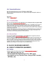
- RF Module: IC3
- PLL Oscillator
- Detector
- Compress/Expander
- Amplifier for transmission and reception

22.2. Power Supply Circuit/Reset Circuit

Circuit Operation:
When power on the Handset, the voltage is as follows;
BATTERY(2.2 V ~ 2.6V: TP3)    TP14(4V)    IC3(6, 27), D3    IC1(37)    IC1(39, 63) (2.65V)
The Reset signal generates R19, C23 and 2.65V.

22.3. Charge Circuit

Circuit Operation:
When charging the handset on the Base Unit, the charge current is as follows;
DC+(5.5V ~ 6V)    D4    R43, R44    (Base)    (Handset)    L4    Q2   F1  

  ... Battery ... BATTERY-    R21    GND    L5    CHARGE-(Handset)   CHARGE-

(Base)    GND    DC-(GND)
In this way, the BBIC on Handset detects the fact that the battery is charged.
The charge current is controlled by switching Q2 of Handset.
Refer to Fig.101 in 

Power Supply Circuit

 ().

22.4. Battery Low/Power Down Detector

Circuit Operation:
"Battery Low" and "Power Down" are detected by BBIC which check the voltage from battery.
The detected voltage is as follows;

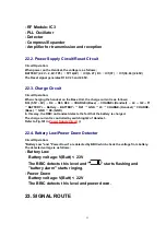
- Battery Low

Battery voltage: V(Batt) < 2.3V

The BBIC detects this level and "

" starts flashing and 

"battery alarm" starts ringing.

- Power Down

Battery voltage: V(Batt) < 2.2V
The BBIC detects this level and power down.

23. SIGNAL ROUTE

51

Summary of Contents for KX-A140EXC

Page 1: ...D400GC KX TCD400GF KX A140EXC KX A140EXF Digital Cordless Phone Dark Blue Version Light Purple Version for Germany SPECIFICATIONS 2003 Panasonic Communications Co Ltd All rights reserved Unauthorized copying and distribution is a violation of law 1 ...

Page 2: ...can also be used Caution PbF solder has a melting point that is 50 F 70 F 30 C 40 C higher than Pb solder Please use a soldering iron with temperature control and adjust it to 700 F 20 F 370 C 10 C In case of using high temperature soldering iron please be careful not to heat too long PbF solder will tend to splash if it is heated much higher than its melting point approximately 1100 F 600 C If yo...

Page 3: ...e manufac turer s specific instructions for the melting points of their products and any precautions for using their product with other materials The following lead free PbF solder wire sizes are recommended for service of this product 0 3mm 0 6mm and 1 0mm 1 2 How to recognize that Pb Free solder is used 1 2 1 Base Unit PCB Component View Flow Solder Side View 1 2 2 Handset PCB Component View Flo...

Page 4: ... the same or equivalent type recommendenced by the manufacturer Dispose of used batteries according to the manufacture s Instructions 4 BATTERY 4 1 Battery Instration Please ensure the batteries are inserted as shown part should be inserted first Close the cover as indicated by the arrow When you replace the batteries part should be removed first 4 2 Battery Charge At the time of shipment the batt...

Page 5: ...y strength 4 3 Battery Life Battery life is dependent on use and conditions but in general when using fully charged Ni MH batteries 700 mAh Talk time 10hrs approx Standby time 120hrs approx When using Ni Cd batteries 250 mAh Talk time 4hrs approx Standby time 40hrs approx Times indicated are for peak performance The batteries reach peak performance after several full charge discharge cycles The ba...

Page 6: ...e telephone socket at this time When replacing the batteries ensure that the correct battery type is selected To exit the operation press any time When Ni Cd batteies are fitted with the setting in icon will disappear and stop charging even if the handset is on the cradle Do not use non rechargeable batteries If no rechargeable batteries are fitted and start charging it may cause the leakage of th...

Page 7: ...5 2 Handset 6 SETTINGS 6 1 Connection Plug in the AC adaptor and the telephone line cord in order 1 2 3 4 7 ...

Page 8: ... must remain connected at all times It is normal for the adaptor to feel warm during use Never install telephone wiring during a lightning storm 6 2 Symbols Used in This Service Manual 6 3 PIN Code 6 3 1 Base Unit 8 ...

Page 9: ...vice Hint If the current 4 digit PIN is forgotten press and you will be able to enter new PIN 6 3 2 Handset To exit the operation press any time For Service Hint If the current 4 digit PIN is forgotten press and you will be able to enter new PIN 9 ...

Page 10: ...stomer cannot register the new handset and may ask to reset the PIN 6 3 3 3 Remedy Preparation Refer to JIGs and PC Connection 1 Solder a pin or lead wire to GND SDA and SCLK on base PCB 2 Plug in AC adaptor to the base 3 Turn on the power to the JIG 9V 4 Then connect the cable to each pins using clip As for the connection between JIG and PCB see below photos PC setting and how to reset base PIN t...

Page 11: ... Unit To exit the operation press any time 1 The factory preset is 0000 6 4 2 Handset You can reset all of the handset settings to their initial settings To exit the operation press any time 1 The factory preset is 0000 11 ...

Page 12: ...cannot be made until key lock is cancelled is displayed and all dialling buttons are locked 6 6 Recall Feature RECALL is used to access special telephone services Contact your Network provider for details If your unit is connected to a PBX pressing RECALL allows you to access some features of your host PBX such as transferring an extension call 6 7 Dialling Pause for PBX line long distance service...

Page 13: ...utside line through a PBX Entering a pause prevents misdialling when you redial or dial a stored number Pressing PAUSE once creates one pause To extend the pause requirement time press PAUSE accordingly 1 is displayed on the LCD 6 8 Call BAR On Off This allows you to make emergency call To exit the operation press any time 1 The factory preset is 0000 2 If is selected is displayed 6 9 Selecting th...

Page 14: ...ial settings however the Phonebook data will be saved 6 10 Summary of Programmable Functions You can select and execute the following functions by pressing direct command as follows without programming These operations need to be done with the Handset near the base unit Press Press or until the arrow points to then press is displayed 1 1 If any key is not pressed over 60 seconds the display will r...

Page 15: ...known working telephone still has problems then please contact the customer service department of your Network provider If it operates correctly then the problem is likely to be a fault in your apparatus In this case contact your supplier for advice Your Network provider may charge you if they attend a service call that is not due to apparatus supplied by them Turn the power OFF then ON Handset Di...

Page 16: ...Cross Reference Power On Off Call BAR On Off Key Lock 8 OPERATIONS 8 1 Power On Off 1 When button is released the display changes to the standby mode 2 The display goes blank 8 2 Making a Call 16 ...

Page 17: ...ng a call 1 You can also answer a call by pressing any dialling button HOLD or 8 4 Setting the Clock Date After a mains power failure the clock needs to be reset Ensure that icon is not flashing To exit the operation press any time 1 For example to set 7 15 enter 0715 2 For example to set the 16th of February 2003 enter 160203 8 5 Phonebook You can store up to 20 caller information in the phoneboo...

Page 18: ...n press RIGHT or LEFT to move cursor then clear a character by pressing CLEAR and or enter characters Characters are cleared or added to the left of the flashing character To enter characters see Character Selection below 2 To continue storing another caller information repeat the steps from 3 18 ...

Page 19: ...e left of the flashing digit If you need to clear or add more than one digit repeat the steps from 5 4 Characters are added to the left of the flashing character If you need to clear or add more than one character repeat the steps from 8 5 To continue clearing another caller information repeat the steps from 2 8 5 2 Storing the Phone Number into the Phonebook When Pre dialling 19 ...

Page 20: ...n press any time 1 If there is no item stored in the redial caller list the display shows 2 If you need correction press RIGHT or LEFT to move cursor then clear a character by pressing CLEAR and or enter digits Digits are cleared or added to the left of the flashing digit 8 5 4 Hot Key Speed Dial You can assign the dialling buttons 1 through 9 as hot keys You can choose 9 phone numbers from the ph...

Page 21: ...no item stored in the phonebook the display shows 2 The number is flashing if the dialling button is already assigned as a hot key 3 Phonebook registration will be remained even hot key registration is cleared 9 DISASSEMBLY INSTRUCUTIONS 9 1 Base Unit 21 ...

Page 22: ... Cabinet Screws 2 6 12 A 2 2 Main P C Board Main P C Board 9 2 Handset Shown in Fig To Remove Remove 3 Rear Cabinet Screws 2 10 B 2 4 Main P C Board Screw 2 8 C 1 4 Main P C Board Screws 2 8 D 2 Main P C Board 10 ASSEMBLY INSTRUCUTIONS 22 ...

Page 23: ...UIDE Flow Chart Cross Reference Check Power Bell Reception Check Battery Charge Check Link Check Handset Transmission Check Handset Reception SIGNAL ROUTE 11 1 Check Power 11 1 1 Base Unit Is the AC Adaptor inserted into AC outlet Check AC Adaptor s specification 23 ...

Page 24: ...Reference Power Supply Circuit Note BBIC is IC2 11 1 2 Handset Cross Reference Power Supply Circuit Reset Circuit Note BBIC is IC1 11 2 Check Battery Charge 11 2 1 Base Unit Cross Reference Charge Circuit 24 ...

Page 25: ...11 2 2 Handset Cross Reference Check Power Charge Circuit Note BBIC is IC1 11 3 Check Link 11 3 1 Base Unit Cross Reference Power Supply Circuit Adjustment 11 3 2 Handset 25 ...

Page 26: ...rence Power Supply Circuit Adjustment 11 4 Check Handset Transmission Cross Reference SIGNAL ROUTE 11 5 Check Handset Reception Cross Reference HOW TO CHECK THE HANDSET SPEAKER SIGNAL ROUTE 11 6 Bell Reception 26 ...

Page 27: ...on 12 1 1 Equipment Required DECT tester Rohde Schwarz CMD 60 is recommended Frequency counter it must be precise to be able to measure 1Hz precision 4ppm Hewlett Packard 53131A is recommended DC power it must be able to output at least 1A current under 9V Digital multi meter DMM it must be able to measure voltage and current Oscilloscope 12 1 2 JIGs and PC 27 ...

Page 28: ...Batch file for setting PQZZTCD410E 12 2 PC Setting 12 2 1 Connections 12 2 2 PC Setting 1 Open a window of MS DOS mode from the start up menu 2 Change a directory to the one with RTX_COM contained 3 Type SET RTX_COM 1 from the keyboard when COM port 1 is used for the connection 4 Type doskey Note See the table below for frequently used commands 28 ...

Page 29: ...3 45 01 23 is address and 45 is data to be written 13 CHECK PROCEDURE HANDSET 13 1 Preparation 13 1 1 Equipment Required DECT tester Rohde Schwarz CMD 60 is recommended Frequency counter it must be precise to be able to measure 1Hz precision 4ppm Hewlett Packard 53131A is recommended DC power it must be able to output at least 1A current under 2 4V for Handset 9V for JIG Digital multi meter DMM it...

Page 30: ...f EEPROM Type rdeeprom 00 00 FF and the data from address 00 00 to FF is read out readid Read ID RFPI Type readid and the registered ID is read out writeid Write ID RFPI Type writeid 00 18 E0 0E 98 and the ID 0018 E0 0E 98 is written setfreq adjust Frequency of RFIC Type setfreq nn nn Getchk Read checksum Type getchk Wreeprom write eeprom Type wreeprom 01 23 45 01 23 is address and 45 is data to b...

Page 31: ...ion sensitivity of base unit is low with noise Make confirmation in item The transmit level is high or low Make adjustments in item The reception level is high or low Make adjustments in item The unit does not link Make confirmation in item Refer to Adjustment 14 1 Adjustment Items Adjustment Point Procedure Check A 2 65V Supply Confirmation 1 Confirm that the voltage between TP187 and GND is 2 65...

Page 32: ...ute the command conttx 3 Input Command rdeeprom_00_00_02 then you can confirm the current value 4 Adjust the frequency of TP1 executing the command setfreq 00 xx where xx is the value so that the reading of the frequency counter is 10 368000MHz 3Hz IC2 IC3 L1 C48 X1 C32 F Hookswitch Check with DC Characteristics 1 Connect J1 Telephone Socket to Tel simulator which is connected with 600 2 Set line ...

Page 33: ...IC2 R32 C2 R23 C80 C1 C13 Q6 R2 R21 R19 R2 C12 D2 C1 C2 R77 D3 R12 Q2 R7 R8 R9 R10 H Transmitted Power Confirmation Remove the Antenna before starting step from 1 to 4 1 Configure the DECT tester CMD60 as follows Setting Testmode FP Traffic Channel 5 Traffic Slot 4 Mode Loopback PMID 0000 2 Execute the command testmode 3 Initiate connection from DECT tester 4 Confirm that the NTP value at ANT is 2...

Page 34: ...2 Adjust the B Field Modulation if required Execute the command readmod and wrtmod xx where xx is the value IC2 IC3 L1 C43 C78 C7 C69 C48 C7 C66 C67 C7 C57 C73 L3 DA1 R66 R6 C55 C56 R7 R79 C54 C5 J Frequency Offset Confirmation Follow steps 1 to 3 of H above 1 Confirm that the frequency offset is 40kHz IC2 IC3 L1 C43 C78 C7 C69 C48 C7 C66 C67 C7 C57 C73 L3 DA1 R66 R6 C55 C56 R7 R79 C54 C5 34 ...

Page 35: ...power to 88dBm 2 Confirm that the BER is 1000ppm IC2 IC3 L1 C43 C78 C7 C69 C48 C7 C66 C67 C7 C57 C73 L3 DA1 R66 R6 C55 C56 R7 R79 C54 C5 L Timing Confirmation Follow steps 1 to 3 of H above 1 Confirm that the Timing accuracy is 5 0ppm IC2 IC3 L1 C43 C78 C7 C69 C48 C7 C66 C67 C7 C57 C73 L3 DA1 R66 R6 C55 C56 R7 R79 C54 C5 35 ...

Page 36: ...vel Confirmation Follow steps 1 to 3 of H above 1 Set DECT tester power to 88dBm 2 Execute the command readrssi 3 Confirm that the returned value is 0x34 A hex IC2 IC3 L1 C43 C78 C7 C69 C48 C7 C66 C67 C7 C57 C73 L3 DA1 R66 R6 C55 C56 R7 R79 C54 C5 36 ...

Page 37: ... 40mA 8 Connect DECT tester to Tel simulator 9 Input audio signal 200mVrms 1kHz tone to Tel simulator DECT tester setting Scramble On AF Gen to ADPCM Off AF Meter Input ADPCM AF Gen Frequency 1000Hz AF Gen Level 200mVrms 10 Confirm hearing tone 360mVrms 60mVrms 11 Adjust audio level if required Make sure current value using getmicgain And then execute the command setmicgain xx where xx is the valu...

Page 38: ...000Hz AF Gen Level 30mVrms 9 Confirm hearing tone 700mV 150mV 10 Adjust audio level if required Make sure current value using getspkrgain And then execute the command setspkrgain xx where xx is the value 11 Confirm that the audio distortion at 600R of Tel simulator is 5 IC2 R32 C2 R23 C80 C1 C13 R22 R2 Q6 R18 R1 R20 C12 D2 C1 C2 R77 R16 D3 R12 Q2 R7 R8 R9 R10 Q3 IC3 L1 C43 C78 C75 C6 C48 C72 C6 C6...

Page 39: ...oes not respond to a call from base unit Make adjustments in item H J N The handset does not transmit or the transmit frequency is off Make adjustments in item H K M The transmit frequency is off Make confirmation in item H K M The transmit power output is low and the operating distance between base unit and handset is less than normal Make confirmation in item The reception sensitivity of base un...

Page 40: ...is 4 1V 0 2V IC1 F1 R21 R4 C33 L2 D1 C15 C2 C14 Q1 R3 R2 D2 R22 C26 X1 C16 B VBACK Status Confirmation 1 Confirm that the voltage between TP18 and GND is 0V 0 4V IC1 F1 R21 R4 C33 L2 D1 C15 C2 C14 Q1 R3 R2 D2 R22 C26 R16 X1 C BBIC Selftest 1 BBIC Selftest Execute the command getchk 2 Confirm the returned checksum value Connection of checksum value and program number is shown below IC1 X1 C16 40 ...

Page 41: ...Confirmation 1 Apply 2 3V 0 005V between TP3 and TP4 2 Execute the command readbatt 3 Subtract 0x06 from returned value which define XX and confirm that the XX is 0x92 0xA2 hex 4 Execute the command WRTBAT2 XX IC1 D4 L4 L5 Q2 Q3 R6 D2 R22 C26 F1 R21 G Battery low Confirmation 1 Apply 2 40V between TP3 and TP4 2 Confirm that there is no Speaker sound Battery low alarm 3 Apply 2 20V between TP3 and ...

Page 42: ...TP value at A201 TP15 is 20dBm 25dBm IC1 IC3 C54 C66 C60 L3 C57 C55 C5 C62 R23 R2 C63 C64 C6 J Modulatoin Check and Adjusment TP15 Follow steps 1 to 4 of I above 1 Confirm that the B Field Modulation is 340kHz div 402kHz div using data type Fig31 2 Adjust the B Field Modulation if required Execute the command Readmod and Writemod xx where xx is the value IC1 IC3 C54 C66 C60 L3 C57 C55 C5 C62 R23 R...

Page 43: ...C5 C62 R23 R2 C63 C64 C6 M Timing Confirmation Follow steps 1 to 4 of I above 1 Confirm that the Timing accuracy is 10ppm IC1 IC3 C54 C66 C60 L3 C57 C55 C5 C62 R23 R2 C63 C64 C6 N RSSI Level Confirmation Follow steps 1 to 4 of I above 1 Set DECT tester power to 88dBm 2 Execute the command readrssi 3 Confirm that the returned value is 0x34 A hex IC1 IC3 C54 C66 C60 L3 C57 C55 C5 C62 R23 R2 C63 C64 ...

Page 44: ...eck and Adjustment TP15 1 Configure the DECT tester CMD60 as follows Setting Testmode FP Mode Normal RFPI 0102030405 2 Execute the command testmode 3 Execute the command regcmd60 4 Initiate connection from DECT tester 5 Execute the command openaudio 6 Confirm that the value of EEPROM address F3F is 02 If the value is not 02 set 02 and power off and power on and return to clause 2 7 Input audio sig...

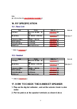
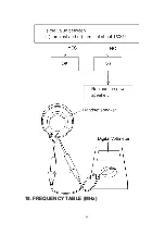
Page 45: ...el 0x34 hex A hex Adjustment M Refer to Adjustment 16 2 Handset Item Value Refer to Remarks TX Power More than 20 dBm 25 dBm Adjustment I Modulation 340 kHz div 402 kHz div Adjustment J Data type Fig31 Frequency Offset 40 kHz 40 kHz Adjustment K RX Sensitivity 1000 ppm Adjustment L Timing Accuracy 10 ppm Adjustment M RSSI Level 0x34 hex A hex Adjustment N Refer to Adjustment 17 HOW TO CHECK THE HA...

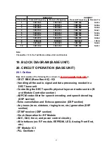
Page 46: ...18 FREQUENCY TABLE MHz 46 ...

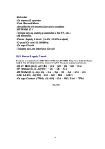
Page 47: ...and Hnadset 19 BLOCK DIAGRAM BASE UNIT 20 CIRCUIT OPERATION BASE UNIT 20 1 Outline Base Unit consists of the following ICs as shown in BLOCK DIAGRAM BASE UNIT DECT BBIC Base Band IC IC2 Handling all the audio signal and data processing needed in a DECT base unit Controlling the DECT specific physical layer and radio section B urst Module Controller section ADPCM codec filter for speech encoding an...

Page 48: ... Charge Circuit Telephone Line Interface Circuit 20 2 Power Supply Circuit The power is supplied to the DECT BBIC RF Module EEPROM Relay Coil LED and Charge Contact from AC Adaptor 6V as shown in Fig 101 The power supply is as follows DECT BBIC IC2 J2 6V D4 Q9 D5 Q8 IC2 RF Module IC3 J2 6V D4 Q9 IC3 EEPROM IC1 J2 6V D4 Q9 D5 Q8 IC2 IC1 LED LED1 J2 6V D4 Q9 R68 LED1 Charge Contact TP84 J2 6V D4 R43...

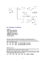
Page 49: ...en the telephone rings the signal is transferred as follows A C4 R2 R29 IC2 DLP BELL CLIP B C3 R1 R30 IC2 DLP BELL CLIP ON OFF hook circuit In the standby mode Q2 is open and connected as to cut the DC loop current and to cut the voice signal The unit is consequently in an off hook condition When IC2 detects a ring signal or press the TALK Key onto the handset Q3 turns on and then Q2 turns on thus...

Page 50: ...from antenna Handset detects the voice signal or data signal in the circuit same as the following explanation of Receiver Block 20 4 2 Receiver Block The signal of 19 2 MHz band 18 81792 MHz 18 97344 MHz which is input from antenna is input to IC3 as shown in BLOCK DIAGRAM BASE UNIT In IC3 the signal of 19 2 MHz band is downconverted to 864 kHz signal and demoduleted and goes to IC2 as DECT frames...

Page 51: ...HARGE Handset L4 Q2 F1 BATTERY Battery BATTERY R21 GND L5 CHARGE Handset CHARGE Base GND DC GND In this way the BBIC on Handset detects the fact that the battery is charged The charge current is controlled by switching Q2 of Handset Refer to Fig 101 in Power Supply Circuit 22 4 Battery Low Power Down Detector Circuit Operation Battery Low and Power Down are detected by BBIC which check the voltage...

Page 52: ...24 CPU DATA BASE UNIT 24 1 IC2 BBIC 52 ...

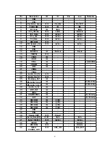
Page 53: ...A I 18 XTAL A I 10 368 MHz 19 VDDLR A I 20 LRB A I 21 VDDA 22 VSSA 23 Audio_Out_N A O 24 Audio_Out_P A O 25 Bandgap_Ref A I 26 Differential_Line_P A I for Bell Clip 27 Differential_Line_N A I for Bell Clip 28 Audio_In_N A I 29 ADC_Ref A I 30 RSSI A I 31 AD2 MPCINP A I for Polarity 32 AD3 A I for Polarity 33 NO USE D I I_PU 34 NO USE D I I_PU 35 NO USE D I I_PU 36 NO USE D I I_PU 37 VDD 38 VSS 39 S...

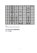
Page 54: ...2 NO USE D I Fixed 53 VSS 54 VDD 55 KEY_IN D I No Key Key 56 NO USE D I O I_PD 57 NO USE D I O I_PD 58 NO USE D I O I_PD 59 NO USE D I O I_PD 60 NO USE D I O I_PD 61 HOOK_CTRL D O Make Break 62 NO USE D I O I_PD 63 ANT1 D O ANT1_ON ANT1_OFF 64 ANT2 D O ANT2_ON ANT2_OFF Note I_PU Internal Pull Up I_PD Internal Pull Down 25 CPU DATA HANDSET 25 1 IC1 BBIC 54 ...

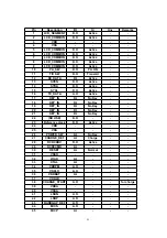
Page 55: ...Active 15 SYCL D O Active 16 TX_DATA A O Active 17 KEY_IN D I No Key 18 KEY_IN D I No Key 19 KEY_IN D I No Key 20 KEY_IN D I No Key 21 KEY_IN D I No Key 22 NO USE D O 23 Reference clock D O Active 24 VDD 25 VSS 26 POWER_SW A I No Key 27 CHARGE_DET A I Charge 28 DCDCDRV D O Active 29 DCDCCMR A I 30 RESET A I Normal 31 VSSO 32 LOAD A I 33 XTAL A I 34 VDDPM A O 35 VDDLO A O 36 VDDBAT A I 37 VDDLR 38 ...

Page 56: ...45 MICP A I 56 ...

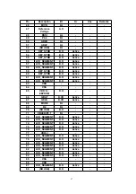
Page 57: ...O Active 62 LCD_SEGMENT D O Active 63 VDD 64 VSS 65 VDD for EEPROM D O 66 I2DAT D I O Active 67 I2CLK D I O Active 68 MODE D I 69 R2 D I 70 NO USE D O 71 VBACK P0 7 D I 72 LCD_SEGMENT D O Active 73 LCD_SEGMENT D O Active 74 LCD_SEGMENT D O Active 75 LCD_SEGMENT D O Active 76 LCD_SEGMENT D O Active 77 VDDLI 78 LCD_SEGMENT D O Active 79 LCD_SEGMENT D O Active 80 LCD_SEGMENT D O Active 81 LCD_SEGMENT...

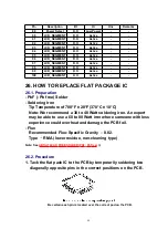
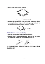
Page 58: ...Preparation PbF Pb free Solder Soldering Iron Tip Temperature of 700 F 20 F 370 C 10 C Note We recommend a 30 to 40 Watt soldering iron An expert may be able to use a 60 to 80 Watt iron where someone with less experience could overheat and damage the PCB foil Flux Recommended Flux Specific Gravity 0 82 Type RMA lower residue non cleaning type Note See ABOUT LEAD FREE SOLDER PbF Pb free 26 2 Proced...

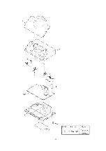
Page 59: ... feeding enough solder to the tip so that it flows under the pins as they are heated 26 3 Modification Procedure of Bridge 1 Add a small amount of solder to the bridged pins 2 With a hot iron use a sweeping motion along the flat part of the pin to draw the solder from between the adjacent pads 27 CABINET AND ELECTRICAL PARTS LOCATION BASE UNIT 59 ...

Page 60: ...60 ...

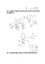
Page 61: ...28 CABINET AND ELECTRICAL PARTS LOCATION HANDSET 29 ACCESSORIES AND PACKING MATERIALS 61 ...

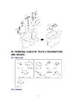
Page 62: ...30 TERMINAL GUIDE OF THE ICs TRANSISTORS AND DIODES 30 1 Base Unit 30 2 Handset 62 ...

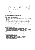
Page 63: ...ning part and product retention After the end of this period the assembly will no longer be available 2 Important safety notice Components identified by the mark indicates special characteristics important for safety When replacing any of these components only use specified manufacture s parts 3 The S mark means the part is one of some identical parts For that reason it may be different from the i...

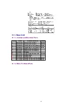
Page 64: ...BODY for KX TCD400GC PS HB 2 PQKM10586Y1 CABINET BODY for KX TCD400GF PS HB 3 PQGT15738Z NAME PLATE for KX TCD400GC 3 PQGT15635Z NAME PLATE for KX TCD400GF 4 PQJT10203Z TERMINAL 5 PQKE10356Z1 GUIDE CHARGE TERMINAL CASE POM HB 6 PQSA10131Z ANTENNA MAIN 7 PQSA10132Z ANTENNA SUB 8 PQYF10560Z2 CABINET COVER for KX TCD400GC PS HB 8 PQYF10560Z1 CABINET COVER for KX TCD400GF PS HB 31 1 2 Main P C Board P...

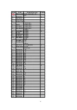
Page 65: ...26Z JACK MODULATOR S J2 K2EZ2B000040 JACK DC RESISTORS R1 ERJ3GEYJ155 1 5M R2 ERJ3GEYJ155 1 5M R3 ERJ3GEYJ224 220K R4 ERJ3GEYJ184 180K R5 ERJ3GEYJ224 220K R6 ERJ3GEYJ184 180K R7 ERJ3GEYJ104 100K R8 ERJ3GEYJ272 2 7K R9 ERJ3GEYJ103 10K R10 ERJ3GEYJ222 2 2K R12 PQ4R18XJ000 0 S R16 ERJ3GEYJ133 13K R18 ERJ3GEYJ392 3 9K R19 ERJ12YJ220 22 R20 ERJ12YJ560 56 R21 ERJ3GEYJ104 100K R22 ERJ3GEYJ333 33K R23 ERJ...

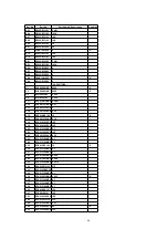
Page 66: ... PQCUV1C474KB 0 47 C13 PQCUV1A105KB 1 C14 PQCUV1C224KB 0 22 C15 ECEA1HKS100 10 S C16 PQCUV1H154KR 0 15 C18 ECUV1H100DCV 10P C19 ECUV1H100DCV 10P C20 ECUV1C104KBV 0 1 C21 ECUV1H100DCV 10P C22 PQCUV1C224KB 0 22 C23 ECUV1C104KBV 0 1 C24 ECUV1C104KBV 0 1 C25 ECEA1CKS100 10 S C26 ECUV1C104KBV 0 1 C27 ECUV1C104KBV 0 1 C28 ECUV1C683KBV 0 068 C29 ECUV1C683KBV 0 068 C30 ECUV1H182KBV 0 0018 C32 ECUV1H270JCV...

Page 67: ...ABS HB 103 PQHS10553Z TAPE DOUBLE SIDE 104 PQHS10554Z SPACER LCD 105 PQBC10375Z1 PUSH BUTTON NAVI 106 PQSX10224S KEYBOARD SWITCH 20KEY for KX TCD400GC 106 PQSX10224T KEYBOARD SWITCH 20KEY for KX TCD400GF 107 PQHS10467Z COVER SP NET 108 L0AD02A00016 SPEAKER 109 PQSA10133Z ANTENNA 110 PQJT10204Z TERMINAL L 111 PQJT10205Z TERMINAL R 112 PQHX11202Z INSULATOR 113 PQJC10058Z BATTERY TERMINAL 114 PQJC100...

Page 68: ...A0072 COIL F1 PQLQR2M5N6K COIL S RESISTORS R1 ERJ3GEYJ222 2 2K R2 ERJ8BQJR30 0 3 R3 ERJ3GEYJ560 56 R4 ERJ3GEYJ103 10K R5 ERJ3GEYJ331 330 R6 ERJ3GEYJ332 3 3K R7 ERJ3GEYJ331 330 R8 ERJ3GEYJ331 330 R11 ERJ3GEY0R00 0 R17 ERJ3GEY0R00 0 R18 ERJ3GEYJ330 33 R19 ERJ3GEYJ153 15K R20 ERJ3GEY0R00 0 R21 ERJ6RSJR10V 0 1 R22 ERJ3GEY0R00 0 R23 ERJ3GEYJ2R2 2 2 R24 ERJ3GEY0R00 0 CAPACITORS C2 ECUV1A475KB 4 7 C3 ECU...

Page 69: ...CUV1H020CCV 2P C66 ECUV1H020CCV 2P OTHERS E101 L0CBAB000052 MICROPHONE E102 PQWLA141E LCD ASS Y X1 H0D103500002 CRYSTAL OSCILLATOR 31 3 Accessories and Packing Materials Ref No Part No Part Name Description Remarks A1 PQLV200CEZ AC ADAPTOR A2 PQJA10139Z CORD TELEPHONE A3 PQQX13611Y INSTRUCTION BOOK A4 PQQW12846W LEAFLET RECHARGE P1 PQPP10100Z PROTECTION COVER for Base Unit P2 PQPP10084Z PROTECTION...

Page 70: ...ers is programmed before the actual hardware fine tuning can be initiated This document lists all default settings with a short description In the tables below values in a range that are similar are not repeated i e Address 00 to 01 contains the value 00 simply means that the value 00 is repeated in all addresses in the range All values in this document are in hexadecimal notation Type Name Descri...

Page 71: ...et is not enrolled 003A 003E FF FF IPUI_3 x D Ipui for handset 3 If set to FF handset is not enrolled 003F 0043 FF FF IPUI_4 x D Ipui for handset 4 If set to FF handset is not enrolled 0044 0048 FF FF IPUI_5 x D Ipui for handset 5 If set to FF handset is not enrolled 0049 004D FF FF IPUI_6 x D Ipui for handset 6 If set to FF handset is not enrolled 004E 008F Reserved x Protocol data 0090 009F UAK_...

Page 72: ...ngMode x D Ring mode Modes used in KAMMA4 20h and 21h Bit 7 5 Mode 001 group 4 Not used 3 0 Id 001 id of first group 32 3 3 BsUiTask settings Address Default Name Country Setting Type Description 0F4B RFPI_1 Config1 01 D BsUiTask configuration MSB Bits 1 enable 0 disable 0 AmPmClockSettingEnabled 1 ClipDetectionSettingEnabled 2 AkzMenuEnabled disabled 3 HakzMenuEnabled disabled 4 RussianClipStting...

Page 73: ...e of the phone e g redial memory at 0311 0392 33 2 Introduction The handset uses a 32k bit serial EEPROM IC2 for storing volatile parameters All parameters are set up before the handset the factory Some of these are vital for the operation of the hardware so a set of default parameters is programmed before the actual hardware fine tuning can be initiated This document lists all default settings wi...

Page 74: ... registration 0107 IPUI_LEN_1 IPUI length for registration 1 0108 0114 IPUI_1 IPUI for registration 1 0115 ZAP_1 ZAP for registration 1 0116 STATUS_1 Status for registration 1 0117 126 UAK_1 UAK for registration 1 0130 134 RFPI_2 RFPI for registration 2 0135 SerClass_2 Service class for registration 2 0136 LAL_2 Location area level for registration 0137 IPUI_LEN_2 IPUI length for registration 2 01...

Page 75: ...4 ZAP for registration 4 01A6 STATUS_4 UAK for registration 4 01A7 01B6 UAK_4 UAK for registration 4 0450 0451 HSPinCode 4 BCD Digits 0462 00 Language 0A D 00 English 01 Spanish 02 French 03 Italian 04 Dutch 05 Turkish 06 Hungarian 07 Portuguese 08 Polish 09 Command 0A German 0467 00 FactoryLanguageSetting 0A D Factory setting for language 00 English 01 Spanish 02 French 03 Italian 04 Dutch 05 Tur...

Page 76: ...step 2 A Bit7 AOG Bit6 AOG2 Bit5 bit0 Gain receive values ranging from 0x00 to 0x30 step representing 1 dB 33 3 5 VolumeSetting Second Block Address Default Name Country Setting Type Description 0F53 FF MenuConfig 20 D bit 0 Registration menu bit 1 Select base menu on bit 2 Internal ringer menu 0 bit 3 Page ringer menu on bit 4 Standby mode menu 0 bit 5 Battery select menu 0 bit 6 Call wating menu...

Page 77: ...37 CIRCUIT BOARD HANDSET 37 1 Component View 37 2 Flow Solder Side View M KXTCD400GC KXTCD400GF KXA140EXC KXA140EXF 77 ...

Page 78: ... 100 80 30 F1 50 5 8 4 1 1 R18 C27 TP18 C20 C23 C18 L5 L4 R21 R6 C24 X1 Q1 C31 TP19 TP13 TP17 TP14 TP16 TP12 TP3 TP4 TP10 BAT GND SCL SDA C57 C64 C56 C55 11 18 1 28 IC3 C60 DECT tester CMD60 I J K L M N O P Frequency Counter H Digital Volt Meter A Digital Volt Meter B C E F H I O P DC 6V Oscilloscope Current Probe D E D D TP5 TP6 TP7 TP8 DC 2 20V 2 40V F G To PC JIG AF SG DECT TESTER CMD60 AF Volt...

Page 79: ...Decoding RF Interface Burst Building Burst Decoding ADPCM Codec Filter EEPROM IC1 SDA SCL SYRI RSSI SYEN RXDA TXDA J2 J1 IC2 IC3 4 0V Reg 2 65V Reg 4 0V 2 65V VUNREG 40 41 28 24 61 9 6 30 11 63 64 6 5 6 4 RF Module 20 30 10 33 Limit Register CHARGE CONTACT 18 16 XTAL 10 368 MHz DTXAF DTXAF 27 26 BBIC Interface ANT1 ANT2 to Tel_Line A B o AC Adaptor ...

Page 80: ...ule ANT BATTERY TERMINAL TP3 TP4 CHARGE CIRCUIT CHARGE CHARGE DETECT SWITCHED SUPPLY CHARGE CONTACTS TP5 4 0V VDDBAT VDDLR SWITCH 31 XTAL 10 368 MHz KEYPAD COLUMNS ROWS LCD 14 Seg Display ON SWITCH 38 27 26 36 37 28 KX A140EXC EXF BLOCK DIAGRAM HANDSET pin 2 5 9 COM 0 5 segment 0 29 pin1 90 100 87 78 84 72 76 61 62 56 58 EARPIECE 42 41 45 17 21 53 55 59 60 34 Burst Encoding Burst Decoding TP6 D3 ...

Page 81: ...7K R8 SA1 100 R30 JMP1 NC JMP3 NC C5 NC C6 NC TP40 R3 220k K0 02 C4 R4 180k 1 5M R1 RLY1 NC NC 1 2 3 4 7 8 9 10 10K R9 K0 022 C3 100K R7 JMP4 NC TP5 33 R43 NC R45 TP84 33 R44 NC C7 4 0V C60 NC Q11 NC NC R70 R71 NC R74 NC R73 NC C62 NC R72 NC L2 NC C63 NC R77 0 J2 1 2 DC_PLUG 5 6M R53 180k R54 K0 01 C49 180k R82 K0 01 C74 5 6M R81 NC C77 NC R85 TP3 TP101 NC JMP8 D7 NC D8 NC LED1 NC Q10 R68 NC OPTIO...

Page 82: ...Q4 NC 750 R28 33K R22 K0 22 C14 K4700P C11 56 R20 TP50 NC R11 Q6 13K R16 C10 NC NC R26 100K R21 R12 0 56 R23 K1 0 C13 NC R14 K0 15 C16 56 R32 K0 22 C22 R38 33 2 65V J101 1 J102 1 J103 1 R52 0 IC3 5 RSSI 6 VCC_OC 7 GND 8 SYCL 9 SYDA 10 SYEN 11 GND 12 RXDSG 13 SYRI 14 GND 15 GND 16 GND 17 GND 18 GND 19 GND 20 RXDA 21 GND 22 GND 23 GND 24 PSEL 25 PAON 26 GND 27 VCC_PA 28 GND 29 GND 30 GND 31 GND 32 G...

Page 83: ...Q4 NC 750 R28 33K R22 K0 22 C14 K4700P C11 56 R20 TP50 NC R11 Q6 13K R16 C10 NC NC R26 100K R21 R12 0 56 R23 K1 0 C13 NC R14 K0 15 C16 56 R32 K0 22 C22 R38 33 2 65V J101 1 J102 1 J103 1 R52 0 IC3 5 RSSI 6 VCC_OC 7 GND 8 SYCL 9 SYDA 10 SYEN 11 GND 12 RXDSG 13 SYRI 14 GND 15 GND 16 GND 17 GND 18 GND 19 GND 20 RXDA 21 GND 22 GND 23 GND 24 PSEL 25 PAON 26 GND 27 VCC_PA 28 GND 29 GND 30 GND 31 GND 32 G...

Page 84: ... 28 C2 K4 7 R4 10K C3 K0 1 S11 S7 S20 S5 S3 S18 S25 S23 S15 S16 S4 S22 S21 S8 S9 C18 K0 1 C20 K0 1 C21 K0 1 C22 K0 1 C23 K0 1 C27 K0 1 R11 0 R21 0 1 F1 S24 S19 S14 S2 S1 CN2 1 C5 2 C4 3 C3 4 C2 5 C1 6 C0 7 S29 8 S28 9 S27 10 S26 11 S25 12 S24 13 S23 14 S22 15 S21 16 S20 17 S19 18 S18 19 S17 20 S16 21 S15 22 S14 23 S13 24 S12 25 S11 26 S10 27 S9 28 S8 29 S7 30 S6 31 S5 32 S4 33 S3 34 S2 35 S1 36 S0...

Page 85: ...62 K1 0 C60 K4 7 R22 0 C63 D10P C64 K1 0 X1 TP13 C55 C2P C56 C2P C54 D10P TP17 TP16 C65 C2P C25 NC D5 NC C66 C2P TP15 IC3 5 RSSI 6 VCC_OC 7 GND 8 SYCL 9 SYDA 10 SYEN 11 GND 12 RXDSG 13 SYRI 14 GND 16 GND 17 GND 18 GND 19 GND 20 RXDA 21 GND 22 GND 23 GND 24 PAON 25 GND 26 GND 27 VCC_PA 28 GND 29 GND 30 GND 31 GND 32 GND 33 RF1 34 GND GND 1 GND 2 GND 3 TXDA 4 CN5 1 SP 2 SP D6 D7 TP19 R24 0 POWER SP ...

Page 86: ...62 K1 0 C60 K4 7 R22 0 C63 D10P C64 K1 0 X1 TP13 C55 C2P C56 C2P C54 D10P TP17 TP16 C65 C2P C25 NC D5 NC C66 C2P TP15 IC3 5 RSSI 6 VCC_OC 7 GND 8 SYCL 9 SYDA 10 SYEN 11 GND 12 RXDSG 13 SYRI 14 GND 16 GND 17 GND 18 GND 19 GND 20 RXDA 21 GND 22 GND 23 GND 24 PAON 25 GND 26 GND 27 VCC_PA 28 GND 29 GND 30 GND 31 GND 32 GND 33 RF1 34 GND GND 1 GND 2 GND 3 TXDA 4 CN5 1 SP 2 SP D6 D7 TP19 R24 0 POWER SP ...

Page 87: ...77 RLY1 C3 C15 LED1 R68 R35 4 1 5 8 R43 R44 R45 A201 A202 L1 R42 R41 R78 R79 Q9 C55 C53 C41 C43 C68 C48 C38 C27 C26 C29 C21 R57 C28 C12 C11 C9 C51 C22 C10 C1 C2 C63 D8 D1 D3 D7 L2 C4 C6 C7 C62 PbF C60 C49 C74 R82 R81 R85 C5 C8 C23 C24 X1 C34 C33 C35 C36 C30 C32 C37 C50 1 L3 C70 C57 C83 C85 C73 C71 C56 28 18 IC3 IC2 IC1 11 64 1 49 33 ANT C66 C72 C58 C54 DA1 C81 C87 C84 C82 C75 C86 C78 C69 C88 C67 C...

Page 88: ...low Solder Side View Q9 Output 4V CHARGE Q9 Input 5 5V TP89 TP188 TP91 TP1 TP97 TP50 TP45 TP40 TP5 1 2 4 6 5 TP90 TP101 TP2 TP3 TP39 TP187 GND VBACK SCL SDA 2 65V TP82 TP84 CHARGE J105 J102 J104 J103 J101 CHARGE PbF RF Clock 10 368MHz CHARGE ...

Page 89: ...C33 MIC R5 R7 R1 D6 C11 R20 R2 R3 C21 C25 R19 D5 IC1 IC2 100 80 30 F1 50 5 8 4 1 1 R18 C27 TP18 C20 C23 C18 L5 L4 R21 R6 C24 X1 Q1 C31 TP19 TP13 TP17 TP14 TP16 TP12 TP3 TP4 TP10 BAT GND SCL SDA C57 C64 C56 C55 11 18 1 28 IC3 C60 SP BBIC 41 SP BBIC 42 TP14 4V RF Clock BBIC 23 10 368 MHz VDD 2 65V CDT BBIC 27 CN3 TP3 KX A140EXC EXF CIRCUIT BOARD HANDSET Component View ...

Page 90: ...KX A140EXC EXF CIRCUIT BOARD HANDSET Flow Solder Side View 1 PROG PbF BOOK UP POWER CAN DOWN RIGHT REDIAL LEFT 1 2 3 6 5 7 0 R 4 9 8 INT MIC TALK 36 CN2 ...

Page 91: ...4 1 5 8 PbF 1 28 18 IC3 IC2 IC1 11 64 1 16 17 32 49 48 33 Marked ...

Page 92: ...TP89 TP188 TP91 TP1 TP97 TP50 TP45 TP40 TP5 1 2 4 6 5 TP90 TP101 TP2 TP3 TP39 TP187 GND VBACK SCL SDA 2 65V TP82 TP84 CHARGE J105 J102 J104 J103 J101 CHARGE PbF Marked ...

Page 93: ...Marked PbF IC1 IC2 100 80 5 8 4 1 50 51 30 31 1 11 18 1 28 IC3 ...

Page 94: ...Marked 1 PROG PbF BOOK UP POWER CAN DOWN RIGHT REDIAL LEFT 1 2 3 6 5 7 0 R 4 9 8 INT MIC TALK 36 CN2 ...

Page 95: ...Clip Base PCB G N D S D A S C L ...

Page 96: ...ft Windows 2000 Version 5 00 2195 C Copyright 1985 2000 Microsoft Corp C cd dect C DECT DOSKEY C DECT SET RTX_COM 1 C DECT initbspin C DECT call wreeprom bat 00 25 00 C DECT call wreeprom bat 00 26 00 C DECT _ ...

Page 97: ...in the cabine CHG terminal comes out of rib by pulling black lead wire when opening the cabinet and turning the PCB over The terminal cannot have enough elastic force cannot have good contact with handset and it will result in charge problem ...

Page 98: ...19 D5 Q10 C18 C20 C25 Q8 Q6 B C E D2 C40 D4 SA1 C77 RLY1 C3 C15 LED1 R68 R35 4 1 5 8 R43 R44 R45 A201 A202 L1 R42 R41 R78 R79 Q9 C55 C53 C41 C43 C68 C48 C38 C27 C26 C29 C21 R57 C28 C12 C11 C9 C51 C22 C10 C1 C2 C63 D8 D1 D3 D7 L2 C4 C6 C7 C62 PbF C60 C49 C74 R82 R81 R85 C5 C8 C23 C24 X1 C34 C33 C35 C36 C30 C32 C37 C50 1 L3 C70 C57 C83 C85 C73 C71 C56 28 18 IC3 IC2 IC1 11 64 1 49 33 ANT C66 C72 C58 ...

Page 99: ...P3 TP39 TP187 GND VBACK SCL SDA 2 65V TP82 TP84 CHARGE J105 J102 J104 J103 J101 CHARGE PbF Frequency Counter E Digital Volt Meter C P To PC JIG Digital Volt Meter Digital Volt Meter D E F G H N O A Digital Volt Meter B DTMF tester Tel Simulator G F O To DECT tester 12Ω 2W ...

Reviews: