The communication with MAIN CPU (IC101) on MAIN board is
established by the serial signals (RXD_232C, TXD_232C) via CN902.
Also, the communication with CDS&AGC (IC801) and Video DSP (IC803)
is established by the serial signals (CS_CDS, SDI_DSP, SDCLK_DSP,
SDO_DSP, SLD_DSP). At the time of CPU (IC902) program upgrade, it is
set to the upgrade mode by BOOT1 and BOOT2 signal in MAIN CPU
(IC101), and the data is transferred via the serial signals (RXD_232C,
TXD_232C) and written.
The timing synchronization with Video DSP (IC803) is performed by
FV_DSP, EP1_DSP and EP2_DSP. The lens control is performed by
signals including PWM connected to the lens board via CN904.
15.1.2.2. Video Signal Process Block
- CDS (IC801)
Power-supply voltages: 3.3V
Package: 36pin QFP
Performs CDS (Correlate Double Sampling) process for CCD output
signal from CCD board, AGC (Auto Gain Control) process and A/D
conversion (10bit)
CCD output signal is sampled with SP1 and SP2 signal to reduce noise
in CDS circuit. Then, after being adjusted to the specified level in
accordance with the serial signal (CS_CDS, SDI_DSP, SDCLK_DSP)
instruction from CAMERA CPU (IC902) in GCA circuit, it is converted to
10bit, the digital signal with the sampling frequency: 14,31818 MHz of
ADCLK input signal by A/D converter. This output signal is adjusted in
order that OB (Optical Black) on CCD output signal shall be standard
level by OBP signal.
- VIDEO DSP (IC803)
Power-supply voltages: +3.3V
Package: 120pin QFP
Clock frequency: 28.636MHz (X801)
Processes CDS IC (IC801) output signal and outputs Y signal and C
signal. Outputs CCD drive signal.
Writing each setting to this IC and reading of data is performed by the
serial signal (CS_CDS, SDI_DSP, SDCLK_DSP, SDO_DSP, SLD_DSP) in
CAMERA CPU.
<Video signal process>
The signal input from CDS IC (IC801) is composed of luminance signal process and color signal
process.
- Luminance signal process
77
Summary of Contents for BB-HCM381CE
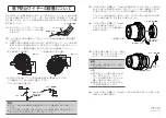
Page 4: ...Lens Board 4...
Page 5: ...Video Board CCD Board 5...
Page 25: ...1 Remove three Screws C And remove the Cabinet Cover 25...
Page 26: ...2 Remove the Screw B And remove the I O Board 26...
Page 29: ...3 Remove eight Screws A 4 Remove the Upper Tilt Cover And remove the Lower Tilt Cover 29...
Page 31: ...4 Remove the Tilt Belt 5 Remove the Tilt Block Ass y Camera Unit 31...
Page 38: ...When fix Lens Board by the Screws please use the jig not to shift Lens Guide Ass y 38...
Page 39: ...10 6 CCD UNIT 39...
Page 49: ...12 TROUBLE SHOUTING 12 1 STARTUP OPERATION 12 2 OTHER FUNCTION CHECK 49...
Page 50: ...12 3 IMAGES BLOCK CHECK 50...
Page 51: ...51...
Page 52: ...12 4 CAMERA UNIT CHECK 52...
Page 53: ...53...
Page 54: ...12 5 LENS PCB CHECK 54...
Page 55: ...55...
Page 56: ...12 5 1 ZOOM Operation Check 56...
Page 57: ...12 6 SOUND BLOCK CHECK 57...
Page 58: ...12 6 1 External Microphone 58...
Page 59: ...12 6 2 Speaker Output 12 6 3 Common Flow for External Microphone and Speaker Output 59...
Page 60: ...12 7 PAN TILT OPERATION CHECK 12 7 1 PAN Operation Check 60...
Page 61: ...12 7 2 TILT Operation Check 61...
Page 62: ...12 8 LAN BLOCK CHECK 62...
Page 63: ...12 9 SD CARD CHECK 63...
Page 64: ...64...
Page 65: ...12 10 POWER SUPPLY BLOCK CHECK 65...
Page 66: ...66...
Page 67: ...12 11 RTC CIRCUIT CHECK 67...
Page 68: ...12 12 I O TERMINAL CHECK 68...
Page 69: ...12 13 LED CIRCUIT CHECK 69...
Page 70: ...12 14 INITIALIZATION OPERATION CHECK 70...
Page 71: ...12 15 VERSION UPGRADE CHECK 71...
Page 94: ...19 ACCESSORIES AND PACKING MATERIALS 94...
Page 95: ...20 REPLACEMENT PARTS LIST Note 1 RTL Retention Time Limited 95...
Page 100: ...C129 ECJ0EF1C104Z 0 1 100...
Page 102: ...C212 ECJ0EC1H101J 100p 102...
Page 104: ...C273 ECJ0EF1C104Z 0 1 104...
Page 106: ...106...
Page 108: ...R104 ERJ3GEYJ101 100 108...
Page 110: ...R235 ERJ3EKF51R1 1 1 110...
Page 116: ...116...
Page 119: ...C939 ECJ0EC1H101J 100p 119...
Page 121: ...R819 ERJ2GEJ101 100 121...
Page 127: ...F501 D4FBR200A003 FUSE 127...
Page 133: ...IC1101 7 1 8 14 BB HCM381 CCD BOARD BOTTOM VIEW...
Page 143: ...C B A D E1 E2...
Page 144: ...F3 F2 G2 E3 F1 G1...
Page 145: ...I1 I2 I3 K1 K2 K3 K4 Tilt Scan L1 L2 M1 M2 H2 H3 H4 H5 J1 J2 J3...
Page 147: ...P6 P7 P8 P9 10Base Hub Connection Communicating Q R1 R2 S1 S2 S3 T1 P5...
Page 148: ...V W1 W3 W4 W2 X1 X2 X3 T2...
Page 149: ...X6 Y4 Y1 Y2 Y3 Z1 Z2 Z3 Z4 X4 X2 X3 X5...
Page 150: ...a1 a2 a3 b1 b2 b3 b4 Pan Scan...