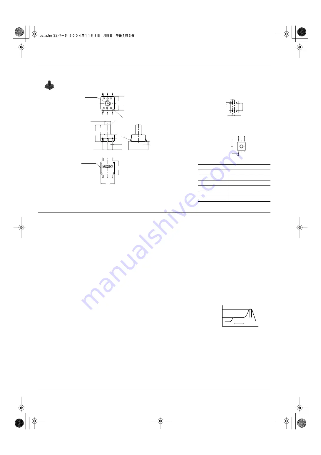
PS-A (ADP5)
4. SMD terminal (Pressure inlet hole: 5mm) ADP52*1
NC
GND NC
Vcc NC Vout
Vcc NC Vout
10.0
±
0.3
.394
±
.012
0.5
.020
JAPAN
.098
±
.010
2.5
±
0.25
.098
±
.010
2.5
±
0.25
0.25
±
0.1
.010
±
.004
NC
GND
NC
T
Y
R
W
Q
E
Atmospheric
pressure
inlet hole
Pressure
inlet hole
2.2 dia.
.087 dia.
R0.2
R
.0
08
3.0
dia.
4-R0.7
4-R.028
0.5
±
0.1
.020
±
.004
0
–0.1
.118
dia.
0
–.004
7.2
.283
7.0
.276
1.8
.071
7.2
.283
7.0
.276
0.15
±
0.1
.006
±
.004
8.5
.335
5.0
.197
Recommended PC board pattern
(TOP VIEW 2:1)
Terminal connection diagram
Terminal No.
Name
1
Vcc (Power supply [+])
2
NC (No connection)
3
Vout (Output)
4
NC (No connection)
5
NC (No connection)
6
GND (Ground)
2.5
.098
2.5
.098
1.1
.043
9.5
.374
1.9
.075
Vcc (5V DC)
Vout
C (0.1
µ
F)
GND
mm
inch
General tolerance: ±0.3
±.012
NOTES
1. Mounting
Use lands on the printed-circuit boards to
which the sensor can be securely fixed.
2. Soldering
Due to its small size, the thermal capacity
of the pressure sensor DIP type is low.
Therefore, take steps to minimize the
effects of external heat.
Damage and changes to characteristics
may occur due to heat deformation.
Use a non-corrosive resin type of flux.
Since the pressure sensor DIP type is
exposed to the atmosphere, do not allow
flux to enter inside.
1) Manual soldering
• Set the soldering tip from 260 to 300°C
(30W), and solder for no more than 5
seconds.
• Please note that output may change if
the pressure is applied on the terminals
when the soldering.
• Thoroughly clean the soldering iron.
2) DIP soldering (DIP terminal type)
• Please keep the DIP solder bath
temperature no higher than 260°C. When
soldering, heat should be applied no
longer than five seconds.
• When mounting onto a PCB of low
thermal capacity, please avoid DIP
soldering as this may cause heat
deformity.
3) Reflow soldering (SMD terminal type)
• The recommended reflow temperature
profile conditions are given below.
• We recommend the screen solder
printing method as the method for cream
solder printing.
• Please refer to the recommended PCB
specification diagram for the PCB foot
pattern.
• Self alignment may not always work as
expected; therefore, please carefully
adjust the position of the terminals and
pattern.
• The profile temperature is the value
measured on the PCB near the terminals.
• When doing reflow soldering on the back
of the PC board after performing sensor
reflow, please fix the sensor with adhesive
and so on.
4) Solder reworking
• Finish reworking in one operation.
• For reworking of the solder bridge, use a
soldering iron with a flat tip. Please do not
add more flux when reworking.
• Please use a soldering iron that is below
the temperature given in the
specifications in order to maintain the
correct temperature at the tip of the
soldering iron.
5) Too much force on the terminals will
cause deformation and loss in
effectiveness of the solder. Therefore,
please avoid dropping and careless
handling of the product.
6) Please control warping of the PCB
within 0.05 mm of the sensor width.
7) When cut folding the PCB after
mounting the sensor, take measures to
prevent stress to the soldered parts.
8) The sensor terminals are designed to
be exposed, so contact of the terminals
with metal shards and the like will cause
output errors. Therefore, please be
careful and prevent things such as metal
shards and hands from contacting the
terminals.
9) To prevent degradation of the PCB
insulation after soldering, please be
careful not to get chemicals on the sensor
when coating.
10) Please consult us regarding the use of
lead-free solder.
3. Connections
1) Please perform connections correctly
in accordance with the terminal
connection diagram. In particular, be
careful not to reverse wire the power
supply as this will cause damage or
degrade to the product.
2) Do not connect terminals that are not
used. This can cause malfunction of the
sensor.
With in
60 sec.
Preheating
Time
Temperature
Peak temperature
150
°
C
302
°
F
230
°
C
446
°
F
(230
°
C
446
°
F
max.
and 10 sec. max.)


