background image


Operation manual for Narrow-pitch connectors A4S


Panasonic Corporation

industrial.panasonic.com/ac/e/ 


©

 Panasonic Corporation 2015 

ACCTF6E-2   201506 


- 16 -


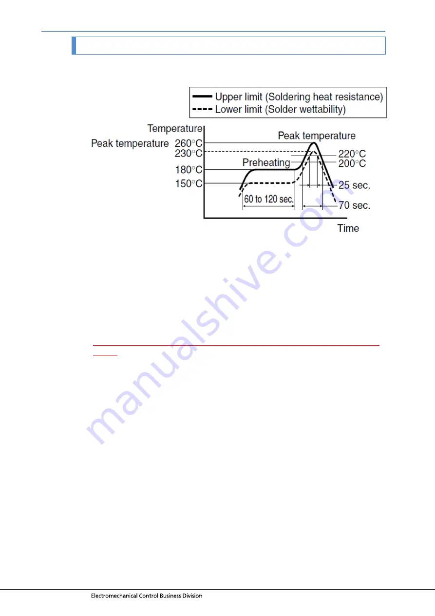
03-2. Precautions for reflow soldering  

(1)Measure the temperature profile at the mounted connector position, and make sure 

that it conforms to the recommended profile.  


(2)When the molded part of connector melts or becomes deformed during the reflow 

process, the heating temperature may be too high, or the connector may be 
affected by a nearby electronic component with high heat capacity.


(3)When the soldering finish is abnormal, check the next points. 
 

If solder creeps to or near the contact section, then excessive solder may have 
been applied or the wicking phenomenon may have occurred. Check the amount 
of solder applied, the position, and the temperature profile at the mounted 
connector position. 


In particular, be careful not to apply excessive solder when the N2 reflow furnace 
is used

.  


(4)Extending the screen pattern outward and providing a solder application position 

on the outer side can help secure a large front fillet.  


(5)In the reflow process of FPC boards, pay attention to the following points to 

reduce temperature variations among connector terminals. 
- Ensure that the FPC board and the base attach firmly to each other when the base 

on which the FPC board is placed is made of metal (e.g., Al). 

- When a metal reinforcing plate is used, further firmly attach the base and 

reinforcing plate (e.g., by using heat-resistant double-sided tape). 


Summary of Contents for A4S

Page 1: ...ACCTF6E 2 2015 06 industrial panasonic com ac e A4S Narrow pitch Connectors onnector Operation manual ...

Page 2: ...al panasonic com ac e Panasonic Corporation 2015 ACCTF6E 2 201506 1 Contents 01 Introduction 2 02 Precautions for product design 3 03 Precautions for mounting and reflow soldering 14 04 Precautions for mating and unmating 20 05 Connectors for inspection and precautions for use 22 ...

Page 3: ...6mm Width 5 0mm Low profile Excellent Very good Very good Mated height 0 8mm Mated height 1 0 1 2mm Mated height 0 9mm Wiring underneath Good Exposed metal part Good Exposed metal part Excellent No exposed metal part Exposed metal part on the rear face Exposed metal part on the rear face Contact reliability Excellent Ultra slim but highly reliable Excellent V notch and double contact Excellent dou...

Page 4: ...e connector in the mounting process Design multi pin connector layouts that do not require a swinging movement during pickup and mounting In many cases deviation of the connector mounting position is caused by the inertia of the swinging movement of the mounter A layout that does not require swinging is thus required Example of a connector layout requiring a swinging movement in the mounting proce...

Page 5: ...or may damage it Pay attention to the following points Cushioning material Casing Sub board flexible board Connector Reinforcing plate Motherboard When an impact such as dropping as shown in the drawing is applied 1 If both boards are not sufficiently fixed the connector will be damaged due to the impact applied to the connector 2 In particular if there is no gap between the casing and sub board A...

Page 6: ... 5 3 To facilitate the mating of connectors we recommend that you pay attention to the following points when designing the motherboard Provide a reference mark Design a layout that allows easy checking of the connector mating condition Flexible board Reinforcing plate Motherboard Provide a reference mark using Silk printing Pattern copper foil ...

Page 7: ...ls for preventing solder from peeling off the terminal Make sure to design a foot pattern for the soldering terminal 3 Pay attention to the following points when providing a through hole by extending the foot pattern If a through hole is created simply by extending the foot pattern by the same width solder is absorbed into the through hole during the reflow process which may cause defective or poo...

Page 8: ...inimum area on the premise that the reflow soldering process is used For manual soldering or for ensuring solder reworkability make a longer pattern at the terminal tip 6 When it is needed to provide pattern wiring and through hole underneath the socket it is possible to use it by designing the pattern as shown below in case insulation underneath the socket is not assured Secure space for applying...

Page 9: ...nEtsu Polymer In case of a one sided FPC board warpage is more likely to occur if a pattern is laid in a line or if the copper foil is applied over the entire FPC board for noise prevention purposes Since the FPC is soft it is difficult to keep it flat Typical transfer jigs for the board mounting process Magic resin Daisho Denshi Keiju board Mitsubishi Resin Assist carrier ShinEtsu Polymer To keep...

Page 10: ...out 30 μm including the adhesive If the thickness exceeds 30 μm design the board so as to remove the coverlay under the connector 3 This connector is often used for connecting the motherboard and FPC board In this case if the FPC board is too short a load that causes deviation will be applied to the connector Make sure to create a design that provides some allowance in the FPC board Connector term...

Page 11: ...y occur depending on the direction the reinforcing plate on material was cut Accordingly make sure to indicate the direction of the material Rolled sheets generate warpage depending on material direction so therefore make sure to warpage reduction into consideration 4 For using an ultra thin reinforcing plate for slimming a product one way is to use metals such as stainless steel for the reinforci...

Page 12: ...g the finish quality in a test run 2 Compared with natural air reflow soldering N2 reflow soldering can reduce oxidization of the melted solder surface This significantly improves the solder wettability Therefore make sure to apply an appropriate amount of solder 3 Do not apply an excessive amount of solder otherwise solder or flux may creep near the contact section and reduce contact reliability ...

Page 13: ...TF6E 2 201506 12 Recommended specifications for PC board and metal mask opening area Applicable product A4S narrow pitch connector socket Recommended PC board pattern Mount pad layout Recommended metal mask pattern When the metal mask thickness is 120 m Terminal section opening area 70 Metal section opening area 100 Insulation area ...

Page 14: ...2015 ACCTF6E 2 201506 13 Recommended specifications for PC board and metal mask opening area Applicable product A4S narrow pitch connector header Recommended PC board pattern Mount pad layout Recommended metal mask pattern When the metal mask thickness is 120 m Terminal section opening area 70 Metal section opening area 100 ...

Page 15: ...ing force g Vacuum pressure mmHG 760 1 033 Nozzle area cm2 Example of machine vacuum pressure setting 480 520 mmHg Picking up the socket 1 The suction area on the socket is 0 7 mm in the shorter direction 2 Dimension of the socket Nozzle tip shape example Single connector weight socket The number of contact 10 20 30 40 50 60 70 80 Weight 0 012 0 017 0 022 0 028 0 033 0 039 0 044 0 050 Socket Picki...

Page 16: ...e connector as shown below 2 Dimension of the header Nozzle tip shape example Single connector weight header The number of contact 10 20 30 40 50 60 70 80 Weight h 0 8mm 0 004 0 007 0 009 0 012 0 014 0 017 0 019 0 021 Weight h 1 0mm 0 005 0 008 0 011 0 014 0 017 0 020 0 023 0 026 Header Picking up face Terminal coplanarity contact and soldering terminals Cross section view Unit mm The number of co...

Page 17: ...on then excessive solder may have been applied or the wicking phenomenon may have occurred Check the amount of solder applied the position and the temperature profile at the mounted connector position In particular be careful not to apply excessive solder when the N2 reflow furnace is used 4 Extending the screen pattern outward and providing a solder application position on the outer side can help...

Page 18: ... 2 During solder rework solder is supplied at and the soldering iron is applied to the tip of each pattern Make sure that solder and the soldering iron do not contact the terminal 3 When carrying out manual soldering or rework avoid using flux if possible in order to prevent it from rising to the contact section For details see the next page 4 When using flux apply as little as possible to the tip...

Page 19: ... Bonkote 2 Selection of soldering iron For narrow pitch connectors with a 0 4 mm pitch we recommend An iron tip with a retractable knife shape Ex Japan Bonkote With a temperature sensor on the iron tip Temperature controllable iron tip It is also necessary to check that there are no differences between the indicated temperature and the actual temperature of the iron tip The following temperatures ...

Page 20: ...or 2 seconds Connector s resistance to soldering heat 300 C 5 sec max 350 C 3 sec max Thin wire solder with a diameter of 0 3 0 4 mm is recommended Final soldering is recommended after provisionally soldering the terminals at both ends Note that when the soldering iron touches the terminal wicking or contact failure may occur 2 Detailed precautions on how to apply the iron tip 3 Flux cleaning meth...

Page 21: ... posts of both connectors are completed A snapping sound will indicate that the simple locking sections are completely mated 4 After completing the mating process check that the clearance between the FPC board and the motherboard is visibly even in both the X and Y directions If the space is not even mating may not be completed Unmate the connectors once check that there is no damage and press the...

Page 22: ...nmating 1 Hold the reinforcing plate at unmating the connector 2 Lift straight up to unmate 3 If the method of unmating described above is not feasible due to a lack of space around the connector please lift around one of the shorter sides of the connector to unmate it Please avoid completely lifting from the other longer side to unmate which risks damaging the connector Lift up ...

Page 23: ... makes mating and unmating works easy Surface treatment contact portion Ni plating on base PdNi Au flash plating on surface improves wear resistant Ordering Connectors for inspection usage Please order with the following part no Characteristics Part no Characteristics Part no Socket Without positioning bosses AXE5E 26 Header Without positioning bosses AXE6E 26 with recommended insertion and remova...

Page 24: ...ach tested object For the purpose of absorbing a positional misalignment on each set the test jig should be equipped with a floating mechanism which can be adjusted in the X Y and axis The floating mechanism should effectively work during insertion Based on the dimensional constraints of the connector insertion guide the inspection jig should be designed to ensure that misalignment during fitting ...

Page 25: ...nectors Prepare a positioning jig for easy alignment Ex Use a positioning pin for alignment Provide a positioning guide for both inspection side and equipment side boards Provide a marking to facilitate easy position alignment by indicating the connector position Ex Provide a connector position marking on the backside of the manually inserted board Ensure that the inspection side connector is manu...

Page 26: ... an ion blow and air blow to remove foreign objects from the connector cavities When forced fitting is repeated under misaligned condition the socket contact may buckle or become deformed Persistence of this condition will push the product side header post and deform it Because this deformation may cause a contact failure the socket must be replaced immediately This condition may indicate a normal...

Page 27: ...ors A4S Panasonic Corporation industrial panasonic com ac e Panasonic Corporation 2015 ACCTF6E 2 201506 26 Amendment history Manual No Date Changes ACCTF6E 1 October 2013 Company name and format change ACCTF6E 2 June 2015 Division name change ...

Page 28: ...ACCTF6E 2 201506 ...

Reviews: