background image

MB-S1

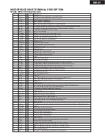
MICROPROCESSOR TERMINAL  DESCRIPTION

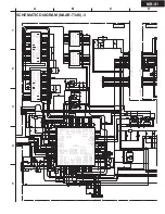
Q7004: MPD70F3033AYGC-8EU

 PIN NO.  FUNCTION  I/O  LOGIC  DESCRIPTION
 1 

SO2 


uPD780232(FL TUBE) Synchronous serial output terminal

 2 

~SCK2 

I/O   

uPD780232(FL TUBE) Synchronous serial CLK terminal

 3 

RXD1 


RS-232C(PHAST) input terminal

 4 

TXD1 


RS-232C(PHAST) output terminal

 5 

~WP/ACC 


MBM29DL (flash ROM) write-protection / acceleration terminal

 6 

EVDD 


An input-and-output port and positive power supply supply for combination functional terminals

 7 

EVSS 


An input-and-output port and grand potential for combination functional terminals

 8 

RY/~BY 


A MBM29DL (flash ROM) ready / busy terminal

 9 

MUTE 

Muting ON/OFF terminal

 10 

SUBMRST 

MB89580 (USB microcomputer) reset terminal (Up (S))

 11 

FLMRST 

uPD780232 (FL microcomputer) reset terminal (Up (S))

 12 

USBHRST 

uPD72012 (USB hub tip) reset terminal (Up (S))

 13 

USBD+ 

USB D+ control terminal (being high pull-up)

 14-16 

A13-A15 


Address bus 13-15

 17 

CIRON/OFF  O 

Circuit power supply ON/OFF

 18 

IC/VPP 


Internal connection (it connects with VSS)

 19-30 

A1-A12 


Address bus 5-12, 1-4

 31 

~RESET 


System reset input

 "32,33" 

"XT1,XT2" 


Oscillation connection for sub clocks

 34 

REGC 


Regulator output stable capacity connection

 "35,36" 

"X2,X1" 


Oscillation connection for main clocks

 37 

VSS 


Ground

 38 

VDD 


Positive power supply terminal

 39 

CLKOUT 


Internal system clock output

 40 

~WRL 

The low rank data light strobe signal terminal of the 16 bit data bus of external

 41 

~UBEN 

The higher rank byte enable signal output terminal of the 16 bit data bus of external

 42 

~WRH 

The higher rank data light strobe signal terminal of the 16 bit data bus of external

 43 

~RD 

The lead strobe signal terminal of the 16 bit data bus of external

 44 

ASTB 


The latch strobe signal output terminal of an external address bus

 45 

CDLED 

CD LED/Program WR Start

 46 

HDDLED 

HDD LED/Program WR Start

 47-54 

D0-D7 

I/O   

Data bus 0-7

 55 

BVDD 


A bus interface and the positive power  supply terminal for combination ports

 56 

BVSS 


A bus interface and the grand terminal for combination ports 

 57-64 

D8-D15 

I/O   

Data bus 8-15 

 65-70 

A16-A21 

I/O   

Address bus 16-21 

 71 

AVDD 


A A/D converter and the analog positive power supply supply terminal for combination ports 

 72 

AVSS 


A A/D converter and the grand terminal for combination ports 

 73 

AVREF 


The standard voltage supply terminal for A/D converters 

 74 


(intact)  (Up (H)) 

 75 

PRVSW1 


Destination distinction switch 1 (temporary) 

 76 

PRVSW2 


Destination distinction switch 2 (temporary) 

 77 

SW1 


Model distinction switch (L:MB-S1 H:HDR -1) 

 78 

SW2 

General-purpose switch 2 (main program forcible download switch) 

 79 

SW3 

General-purpose switch 3 (for an external ROM/RAM check) 

 80-85 


(intact)  (Up (H)) 

 86 

NMI 


"The terminal for power failure detection (it will input, by the time it will fall completely, if voltage begins to fall) "

 87 

FROMA0 


(intact)  

 88 

D_MUTE 


Digital output muting terminal (Up (H)) 

 89 

FLRDY 

FL microcomputer data ready input terminal 

 90 

ELVOL1 


Electronic volume control terminal 1 

 91 

ELVOL2 


Electronic volume control terminal 2 

 92 

ELVOL3 


Electronic volume control terminal 3 

 93 

GAIN_CTL 


GAIN CTL port

 94 

SDA0 


I2 C-bus terminal for QPICT board connection (DATA LINE) (Up (H)) 

 95 

QPINT 

Interrupt QPICT board signal terminal 

 96 

SCL0 


I2 C-bus terminal for QPICT board connection (CLK LINE) (Up (H)) 

 97 

RXD0 


MB89580 (USB sub microcomputer) asynchronous serial input terminal 

 98 

TXD0 


MB89580 (USB sub microcomputer) asynchronous serial output terminal 

 99 

QPRST 

QPICT reset signal terminal 

 100 

SI2 


uPD780232 (FL microcomputer) synchronous serial input terminal

Summary of Contents for MB-S1

Page 1: ... REC REC MODE EXTERNAL INPUT FAVORITE IT CD HDD SAFETY RELATED COMPONENT WARNING COMPONENTS IDENTIFIED BY MARK ON THE SCHEMATIC DIAGRAM AND IN THE PARTS LIST ARE CRITICAL FOR RISK OF FIRE AND ELECTRIC SHOCK REPLACE THESE COMPONENTS WITH ONKYO PARTS WHOSE PART NUMBERS APPEAR AS SHOWN IN THIS MANUAL MAKE LEAKAGE CURRENT OR RESISTANCE MEASUREMENTS TO DETERMINE THAT EXPOSED PARTS ARE ACCEPTABLY INSULA...

Page 2: ...ith Audio CD Playback only 1 USB Type B 1 RS 232C Dsub 9pin Frequency Response 5Hz 20 kHz Playback Harmonic distortion 0 007 at 1kHz 0dB Playback Dynamic range 90 dB Playback Signal to noise ratio 90 dB Recording Harmonic distortion LPCM 0 007 at 1kHz 0dB MP3 0 018 at 1kHz 0dB Recording Dynamic range 90dB Recording Signal to Noise ratio 90dB Channel Separation 90dB playback Wow and Flutter Below t...

Page 3: ...d There is no text data or undefined name in the current track Clock Adjust The clock of this unit has not been set Copy Protect An attempt was made to record copyright protected material Group Full An attempt was made to record more than 999 groups HDD Check System error occurred Wait for a while HDD Check 999 System error occurred Do not operate the MB S1 until the count down is over HDD Media F...

Page 4: ...raphy mode 13 SSCBJ I L SSC rotary encoder pulse input terminal Z Z Z Z 14 SSCAJ I H SSC rotary encoder pulse input terminal Z Z Z Z 15 IRMZ I L Remote control 1 ZONE2 signal input terminal Active L Z Z Z Z 16 FAVORITE O FAVORITE Light Emitting Diode output terminal 17 STBYLED O STANDBY RECEIVED output terminal 18 GND The GND terminal of a A D converter 19 22 K3 K0 I A Main part key input terminal...

Page 5: ...the 16 bit data bus of external 44 ASTB O The latch strobe signal output terminal of an external address bus 45 CDLED O H CD LED Program WR Start 46 HDDLED O H HDD LED Program WR Start 47 54 D0 D7 I O Data bus 0 7 55 BVDD A bus interface and the positive power supply terminal for combination ports 56 BVSS A bus interface and the grand terminal for combination ports 57 64 D8 D15 I O Data bus 8 15 6...

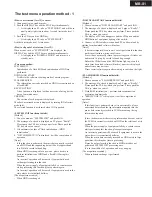
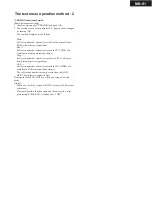
Page 6: ...if equipment is used in the state where it is initialized halfway The use pattern assumed When HDD is exchanged DOWNLOAD START functional details Methode 1 Choose a menu as DOWNLOAD START and push JOG 2 The message of a check is displayed on FL pipe as Really Please push the YES key when you perform Please push the NO key when you cancel 3 The display of FL tube disappears and the CD button and th...

Page 7: ...y recorded in CPU V850 of a main board starting processing charge Disp Soft version number currently recorded on CPU of a display board display processing charge USB Soft version number currently recorded in CPU MB89 of a main board USB communication charge The soft version number currently recorded on the QP B QPICT board device control charge Please push the MENU EXIT key when you escape from th...

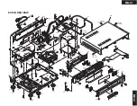
Page 8: ...T P A34 D A35 T P A34 D A35 T P A34 D A35 T P A32 E4 U2 A18 Z3 A27 U5 U1 U8 U7 A30 E2 E1 A26 A26 A26 A26 A24 A15 A39 Z5 Z6 Z6 Z5 A36 A36 A36 A36 A36 Z4 Z4 A24 Z6 Z6 A20 A37 F9001 E8 E5 Z2 A23 A28 A38 A37 A37 E6 U4 A5 A37 A13 A11 A34 A34 A33 A8 A29 A31 A19 A9 A12 A14 A2 A10 A4 A34 A37 A21 A25 A1 A16 A17 A17 A16 A16 A16 U3 Z1 U6 A22 ...

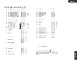
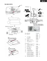
Page 9: ...ANDBY 28198930 A12 FACET FAVORITE 28198940 A13 GUIDE STANDBY 27268049 D 27268047 T 27268048 P A14 GUIDE STOP 27268053 D 27268057 T 27268058 P A15 REAR PANEL 27122920 D 27122919 T P A16 BOTTOM LEG AS 27175388 A17 CUSHION SHLD 28141490 No Description Part number A18 CUSHION 28141491 A19 CUSHION 28141486 A20 CUSHION 28141467 A21 HOLDER KGLS 18RF 27190657 A22 HOLDER KGPS 18RF 27190926 A23 HOLDER KGLS ...

Page 10: ...R 4 3 0 4 4 7 R 4 6 0 8 1 0 K R 4 6 0 9 4 7 R 4 6 0 3 1 0 K R 4 0 3 3 4 7 K R 4 0 0 2 1 2 0 R 3 0 0 3 4 7 R 3 0 0 2 4 7 R 3 0 0 4 4 7 R 3 0 0 1 4 7 R 4 0 0 7 0 R 4 5 5 6 1 0 R 4 5 5 5 1 0 R 4 5 3 8 2 2 K R 4 5 5 0 1 0 R 4 5 4 9 1 0 R 4 5 2 8 0 R 4 5 4 7 1 0 R 4 5 4 8 1 0 R 4 3 1 9 4 7 R 4 6 0 4 0 R 4 5 3 9 4 7 R 4 5 4 0 2 2 K R 4 5 4 1 3 3 R 4 5 4 2 3 3 R 4 9 0 1 0 R 4 9 0 3 0 R 4 9 0 2 1 K R 4 9 ...

Page 11: ... 1 0 4 Z C 3 0 1 2 1 0 4 Z C 3 0 1 0 1 0 4 Z C 4 1 0 7 1 0 1 C 4 1 0 8 1 0 1 C 3 0 0 2 1 0 4 Z C 3 0 0 5 1 0 4 Z C 3 0 0 3 1 0 4 Z C 3 0 0 7 1 0 4 Z C 3 0 0 8 1 0 1 C 3 0 0 6 4 7 0 C 4 0 0 9 1 0 4 Z 3 3 0 C 4 0 0 2 3 3 0 R 4 0 3 2 0 R 4 0 3 1 0 R 4 0 0 9 1 0 R 4 1 2 0 R 4 1 1 9 R 4 0 1 0 1 0 R 4 5 1 9 0 R 4 5 5 8 1 0 R 4 5 5 7 1 0 R 4 5 0 1 1 0 0 R 4 5 4 4 4 7 K R 4 5 0 6 8 2 K R 4 5 4 5 2 7 K R 4...

Page 12: ... Y B O A R D P 7 5 0 1 F R O M C P U B O A R D D 7 0 0 9 C R S 0 8 D 7 0 0 2 1 S S 3 5 2 L 7 0 0 1 B L M 2 1 P 2 2 1 S G C 7 0 4 3 0 1 C 7 0 2 6 2 2 5 0 C 7 0 2 8 2 2 5 0 C 7 0 3 5 2 2 5 0 C 7 0 1 0 1 0 0 6 3 C 7 0 3 0 1 5 0 C 7 0 0 9 1 0 0 6 3 C 7 0 1 6 1 0 0 6 3 C 7 5 0 1 1 0 0 6 3 C 7 0 2 3 1 0 0 6 3 C 7 0 0 7 1 0 0 6 3 C 7 0 4 9 1 0 0 6 3 C 7 0 1 8 1 0 0 6 3 C 7 0 5 0 1 0 0 6 3 C 7 0 3 1 1 0 0...

Page 13: ... P 3 6 P 4 4 4 2 F I P 3 7 P 4 5 4 1 F I P 4 7 6 F I P 4 1 P 5 1 3 7 F I P 4 2 P 5 2 3 6 F I P 4 3 P 5 3 3 5 F I P 4 4 P 5 4 3 4 F I P 4 5 P 5 5 3 3 F I P 4 6 P 5 6 3 2 F I P 4 7 P 5 7 3 1 F I P 4 8 P 6 0 3 0 F I P 4 9 P 6 1 2 9 F I P 5 7 5 F I P 5 0 P 6 2 2 8 F I P 5 1 P 6 3 2 7 F I P 5 2 P 6 4 2 6 F I P 6 7 4 F I P 7 7 3 F I P 8 7 2 F I P 9 7 1 I C V P P 5 P 0 0 I N T P 0 1 5 P 0 1 I N T P 1 1 6...

Page 14: ... 1 7 0 2 2 1 2 W R 9 0 1 6 1 0 1 2 W R 9 0 1 5 0 2 2 1 2 W R 9 0 1 4 0 2 2 1 2 W R 9 0 1 3 0 2 2 1 2 W R 9 0 1 2 1 1 2 W R 9 0 1 1 1 1 2 W R 9 0 0 8 4 7 K 2 W R 9 0 0 5 5 6 K 1 2 W R 9 0 0 9 1 K 1 2 W R 9 0 0 4 6 8 0 1 2 W R 9 0 1 0 4 7 1 2 W R 9 0 0 7 1 K 1 2 W R 9 0 0 3 6 8 K 2 W R 9 0 0 1 0 2 2 5 W D O C P F B C O N T V C C G N D S Q 9 0 0 1 S T R F 6 6 7 6 3 1 5 2 4 D 9 0 2 3 A G 0 1 Z D 9 0 0...

Page 15: ... A I N S T F I R E H A Z A R D R E P L A C E F O R C O N T I N U E D P R O T E C T I O N A N D R A T I N G I N D I C A T E D O N L Y W I T H F U S E O F S A M E T Y P E C A U T I O N Q 9 0 0 3 S I 3 1 2 0 C G N D 1 O N 2 S 4 V I 5 V O 3 Q 9 0 0 4 S I 3 1 2 0 C G N D 1 O N 2 S 4 V I 5 V O 3 Q 9 0 0 7 S E 0 0 5 N 2 3 1 D 9 0 2 0 U D Z S 3 6 B D 9 0 2 2 U D Z S 5 6 B Q 9 0 0 6 2 S A 9 5 0 Y C 9 0 4 2...

Page 16: ...7 0 2 2 1 2 W R 9 0 1 6 1 0 1 2 W R 9 0 1 5 0 2 2 1 2 W R 9 0 1 4 0 2 2 1 2 W R 9 0 1 3 0 2 2 1 2 W R 9 0 1 2 1 1 2 W R 9 0 1 1 1 1 2 W R 9 0 0 8 4 7 K 2 W R 9 0 0 5 5 6 K 1 2 W R 9 0 0 9 1 K 1 2 W R 9 0 0 4 6 8 0 1 2 W R 9 0 1 0 4 7 1 2 W R 9 0 0 7 1 K 1 2 W R 9 0 0 3 6 8 K 2 W R 9 0 0 1 0 2 2 5 W D O C P F B C O N T V C C G N D S Q 9 0 0 1 S T R F 6 6 7 6 3 1 5 2 4 D 9 0 2 3 A G 0 1 Z D 9 0 0 8 ...

Page 17: ...G A I N S T F I R E H A Z A R D R E P L A C E F O R C O N T I N U E D P R O T E C T I O N A N D R A T I N G I N D I C A T E D O N L Y W I T H F U S E O F S A M E T Y P E C A U T I O N Q 9 0 0 3 S I 3 1 2 0 C G N D 1 O N 2 S 4 V I 5 V O 3 Q 9 0 0 4 S I 3 1 2 0 C G N D 1 O N 2 S 4 V I 5 V O 3 Q 9 0 0 7 S E 0 0 5 N 2 3 1 D 9 0 2 0 U D Z S 3 6 B D 9 0 2 2 U D Z S 5 6 B Q 9 0 0 6 2 S A 9 5 0 Y C 9 0 4 ...

Page 18: ...Y CARD 29365083B D P9 REMOTE CONTROL UNIT RC 459P 24140459 P10 BATTERY UM 3 3010054 P11 PIN CORD AS or 2010098A or PIN CORD AS 2010326 P12 CORD AS RI 2010200 P13 CD ROM MB S1 292174A P14 CORD AS USB 1M 2010391 P15 CV PLUG CV K 2 25055911 T P16 INS MANUAL E MB S1 29343221A INS MANUAL Ct MB S1 29343223 T INS MANUAL G MB S1 29343275 P INS MANUAL F MB S1 29343276 P INS MANUAL I MB S1 29343277 P P17 IN...

Page 19: ...9010 D9011 D9012 D9013 D9014 D9015 D9016 D9018 D9019 D9021 D9023 E9001 L9009 L9009 L9002 L9003 L9003 L9004 L9004 L9005 L9005 L9006 L9006 L9007 L9007 L9008 L9008 P9001 P9002 P9002 P9003 P9003 P9004 P9004 P9005 P9006 P9007 Q9001 Q9001 Q9002 Q9002 Q9003 Q9003 Q9004 Q9004 Q9005 Q9005 Q9006 Q9007 R9001 R9002 R9003 R9004 R9005 R9006 R9007 R9008 R9009 R9010 R9011 R9012 R9013 R9014 R9015 R9016 R9017 R9019...

Page 20: ...501 R7502 R7503 R7504 R7505 R7506 R7507 R7508 R7509 R7510 R7511 R7512 R7513 R7514 R7515 R7516 R7517 R7518 R7519 R7520 R7521 R7522 R7523 R7524 R7525 R7526 R7527 R7528 R7529 R7530 R7532 R7533 R7534 R7536 R7537 R7538 R7540 R7541 R7542 R7543 R7544 R7545 R7546 X7501 R7547 R7548 R7549 R7550 R7551 R7552 R7553 R7554 R7555 R7556 R7557 R7558 R7559 R7560 R7561 R7562 R7563 R7564 R7565 R7566 R7567 R7568 R7569 ...

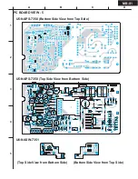
Page 21: ...0 Q7020 R7093 R7094 R7114 NCETC 7347 25137347 0 1 10 11 20 L7008 L7009 L7010 P7004 P7012 P7012 NCETC 7348 ONKYO 25137348 3 R7102 MB S1 PC BOARD VIEW 3 MB S1 U2 NAETC 7347 Top Side View from Bottom Side U2 NAETC 7347 Bottom Side View from Top Side U3 NAETC 7348 Top Side View from Bottom Side U3 NAETC 7348 Bottom Side View from Top Side ...

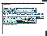
Page 22: ...A 1 2 3 4 B C D E P4302 P4302 MB S1 PC BOARD VIEW 2 U1 NAAR 7346 Bottom Side View from Top Side MB S1 ...

Page 23: ...C4542 C4543 C4544 C4545 C4547 C4548 C4551 C4552 C4601 C4602 C4603 C4604 C4901 C4902 C4903 C4904 C4905 C4906 C4907 C4908 C4909 C4910 C4911 C4912 C4913 C4914 D4601 D4602 D4603 E4301 E4302 E4303 E4304 E4305 E4306 L3001 L3002 L3003 L3004 L4001 L4002 L4501 L4502 L4503 L4504 P3001 P3002 P3002 P3003 P3003 P4101 P4101 P4201 P4201 P4901 Q3001 Q3001 Q3002 Q3002 Q3003 Q3003 Q4001 Q4001 Q4002 Q4002 Q4003 Q410...

Page 24: ...AL HC 49 U03 4MHz 3010350 CAPACITOR C7043 EDL C DX 5R5L104 3000078 C4003 ELECT C CE04W6 3V 470M 354724719 C4027 C4028 ELECT C CE04W16V 470M 354744719 C4536 C4603 ELECT C CE04W6 3V 470M 354724719 C4019 C4020 TF C ECQ B50V 222J 374722224 C4021 C4022 TF C ECQ B50V 102J 374721024 C4023 C4024 TF C ECQ B50V 472J 374724724 C No Description Part number RESISTOR R7108 RESISTOR miniSMDC100 4000192R2 SW TRM ...

Page 25: ...31 T P RESISTOR R9001 METAL PR MPC74 5WK 0 22 4000076 R9002 METAL O R RS2WBJ 0 22 441722294F R9003 METAL O R RS2WBJ 68K 441726834NF R9004 METAL O R RS1 2WBJ 680 443526814 R9005 METAL O R RS1 2WBJ 5 6K 443525624 R9007 METAL O R RS1 2WBJ 1K 443521024 R9008 METAL O R RS2WBJ 47K 441724734F R9009 METAL O R RS1 2WBJ 1K 443521024 R9010 METAL O R RS1 2WBJ 47 443524704 R9011 R9012 METAL R RNU1 2WCJ 1 45353...

Page 26: ...GmbH Industriestrasse 20 82110 Germering GERMANY Tel 089 849 320 Fax 089 849 3265 E mail info onkyo de ONKYO CHINA LIMITED Units 2102 2107 Metroplaza Tower I 223 Hing Fong Road Kwai Chung N T HONG KONG Tel 852 2429 3118 Fax 852 2428 9039 Sales Product Planning Div 2 1 Nisshin cho Neyagawa shi OSAKA 572 8540 JAPAN Tel 072 831 8111 Fax 072 833 5222 ONKYO CORPORATION PN 0M3710 Printed in Japan ...

Page 27: ......

Reviews: