


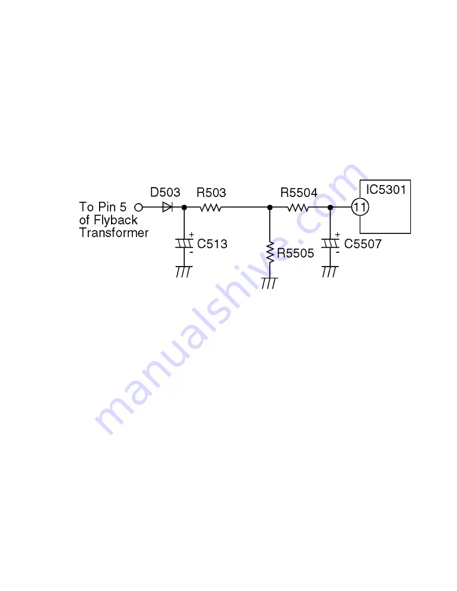
HORIZONTAL OSCILLATOR DISABLE CIRCUIT
The positive DC voltage, supplied from the D503 cathode for monitoring high voltage,
is applied to the IC5301 Pin11 through R503 and R5504. Under normal conditions, the
voltage at IC5301 Pin 11 is less than approx 3 V. If the high voltage at Flyback Tr Pin 5
exceeds the specified voltage, the positive DC voltage which is supplied from the
D503 cathode also increases. The increased voltage is applied to IC5301 Pin11
through R503 and R5504. Due to the increased voltage at IC5301 Pin11, the horizontal
oscillator frequency increases, the picture goes out of horizontal sync, the beam
current decreases and the picture becomes dark in order to keep X-radiation under
specification.
Figure 3
3. PREVENTION OF ELECTROSTATIC DISCHARGE
(ESD) TO ELECTROSTATICALLY SENSITIVE (ES)
DEVICES
Some semiconductor (solid state) devices can be damaged easily by static electricity.
Such components commonly are called Electrostatically Sensitive (ES) Devices.
Examples of typical ES devices are integrated circuits and some field-effect
transistors are semiconductor "chip" components. The following techniques should
be used to help reduce the incidence of component damage caused by electrostatic
discharge (ESD).
1. Immediately before handling any semiconductor component or
semiconductor-equipped assembly, drain off any ESD on your body touching a
known earth ground. Alternatively, obtain and wear a commercially available
discharging ESD wrist strap, which should be removed for potential shock
reasons prior to applying power to the unit under test.
2. After removing an electrical assembly equipped with ES devices, place the
assembly on a conductive surface such as aluminum foil, to prevent electrostatic
charge buildup or exposure of the assembly.
3. Use only a grounded-tip soldering iron to solder or unsolder ES devices.
6
Summary of Contents for PVQ-1300W
Page 9: ...Fig 1 3 Fig 1 4 9...
Page 10: ...10...
Page 13: ...5 1 2 1 2 Service Position 2 Fig 2 2 13...
Page 18: ...18...
Page 31: ...5 2 1 HOW TO READ THE IDENTIFICATION MARK OF CHIP COMPONENTS 31...
Page 34: ...6 1 2 Disassembly Method 34...
Page 35: ...35...
Page 37: ...Fig D4 37...
Page 38: ...Fig D5 38...
Page 43: ...6 2 2 Inner Parts Location Fig J1 1 43...
Page 44: ...6 2 3 EJECT Position Confirmation Fig J1 2 44...
Page 45: ...6 2 4 Grounding Plate Unit Full Erase Head and Cylinder Unit Fig J2 1 45...
Page 46: ...46...
Page 48: ...6 2 5 Capstan Belt Support Angle Intermediate Gear B and Main Cam Gear Fig J3 1 48...
Page 49: ...49...
Page 56: ...6 2 7 Reel Gear and Main Rod Fig J5 1 56...
Page 58: ...6 2 8 Stopper Angle Capstan Rotor Unit Oil Seal Capstan Stator C B A and MR Head Fig J6 1 58...
Page 59: ...59...
Page 61: ...61...
Page 65: ...6 2 10 1 Reassembly Notes 65...
Page 71: ...6 3 CASSETTE UP ASS Y SECTION 71...
Page 72: ...6 3 1 Top Plate Wiper Arm Unit and Holder Unit Fig K1 1 72...
Page 73: ...73...
Page 75: ...75...
Page 77: ...7 ADJUSTMENT PROCEDURES 7 1 SERVICE FIXTURES AND TOOLS 77...
Page 94: ...94...
Page 117: ...8 SCHEMATIC DIAGRAMS 8 1 SCHEMATIC DIAGRAM AND CIRCUIT BOARD LAYOUT 117...
Page 132: ...DIODES 132...
Page 139: ...CAPACITORS 139...


